Photoelectric conversion element, method for manufacturing same, and imaging apparatus

a technology of photoelectric conversion elements and manufacturing methods, which is applied in the direction of sustainable manufacturing/processing, television systems, and controlled devices, etc., can solve the problem of reducing the sensitivity of the photoelectric conversion elements from red to near-infrared wavelength regions, unable to detect infrared light having a wavelength of 1.1 m or greater in principle, and unable to achieve the effect of less likelihood and reliable address of miniaturization

Active Publication Date: 2020-04-07
SONY CORP
View PDF19 Cites 1 Cited by
  • Summary
  • Abstract
  • Description
  • Claims
  • Application Information

AI Technical Summary

Benefits of technology

[0066]In the photoelectric conversion elements of the present technology, the photoelectric conversion elements constituting the imaging apparatus of the present technology, and the photoelectric conversion elements manufactured by the methods for manufacturing the photoelectric conversion elements according to the first to sixth aspects of the present technology, the element isolation layer surrounds the lateral surface of the photoelectric conversion layer. Therefore, there is no fear (less likelihood) of causing a crystal defect or the like when forming a region that divides the adjacent photoelectric conversion elements, and miniaturization can be reliably addressed. Note that effects described in the present specification are given only for exemplification purpose and the present specification is not limited to the effects but may include additive effects.

Problems solved by technology

However, the increase in the aspect ratio of the photoelectric conversion elements causes a problem such as inter-pixel color mixture in which light incident on another photoelectric conversion element adjacent to one photoelectric conversion element is also incident on the one photoelectric conversion element.
When the aspect ratio of the photoelectric conversion elements is decreased to reduce the inter-pixel color mixture, a problem such as reduction in the sensitivity of the photoelectric conversion elements from red to the near-infrared wavelength region is caused.
In addition, Si cannot detect infrared light having a wavelength of 1.1 μm or greater in principle since its band gap energy is 1.1 eV.

Method used


Image

  • Photoelectric conversion element, method for manufacturing same, and imaging apparatus
  • Photoelectric conversion element, method for manufacturing same, and imaging apparatus
  • Photoelectric conversion element, method for manufacturing same, and imaging apparatus

Examples


first embodiment

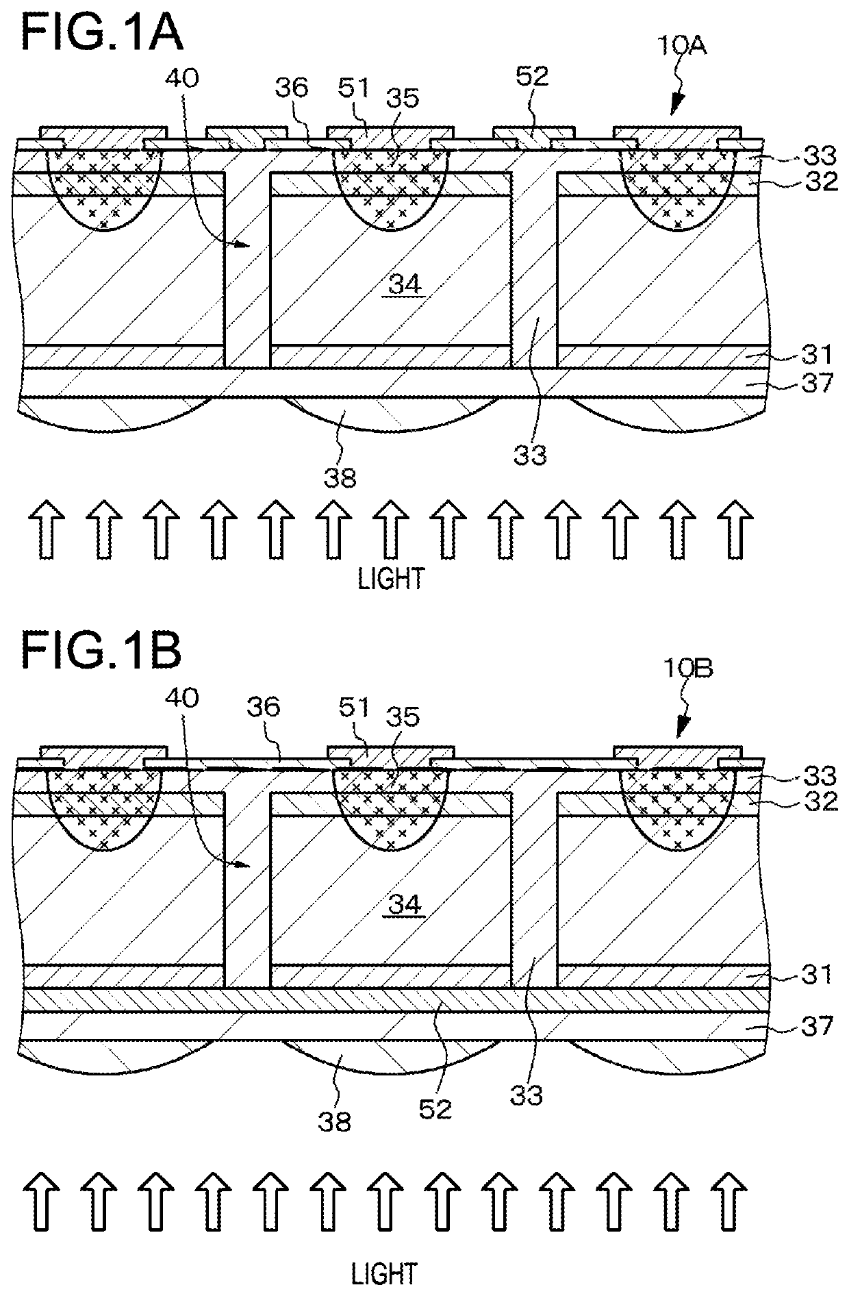
[0180]A first embodiment relates to a photoelectric conversion element (a light-receiving element, a photodiode, or an imaging element) of the present technology, a method for manufacturing a photoelectric conversion element according to a first aspect of the present technology, and an imaging apparatus of the present technology. FIG. 1A shows a schematic partial cross-sectional view of the photoelectric conversion element of the first embodiment. In addition, FIG. 4A schematically shows the arrangement of a first electrode, a second electrode, a second compound semiconductor layer, an element isolation layer, and a recess part in the photoelectric conversion element of the first embodiment, FIG. 5 schematically shows the connection between the photoelectric conversion element of the first embodiment and a driving substrate, and FIG. 6 shows a conceptual diagram of the imaging apparatus of the first embodiment.

[0181]A photoelectric conversion element 10A of the first embodiment incl...

second embodiment

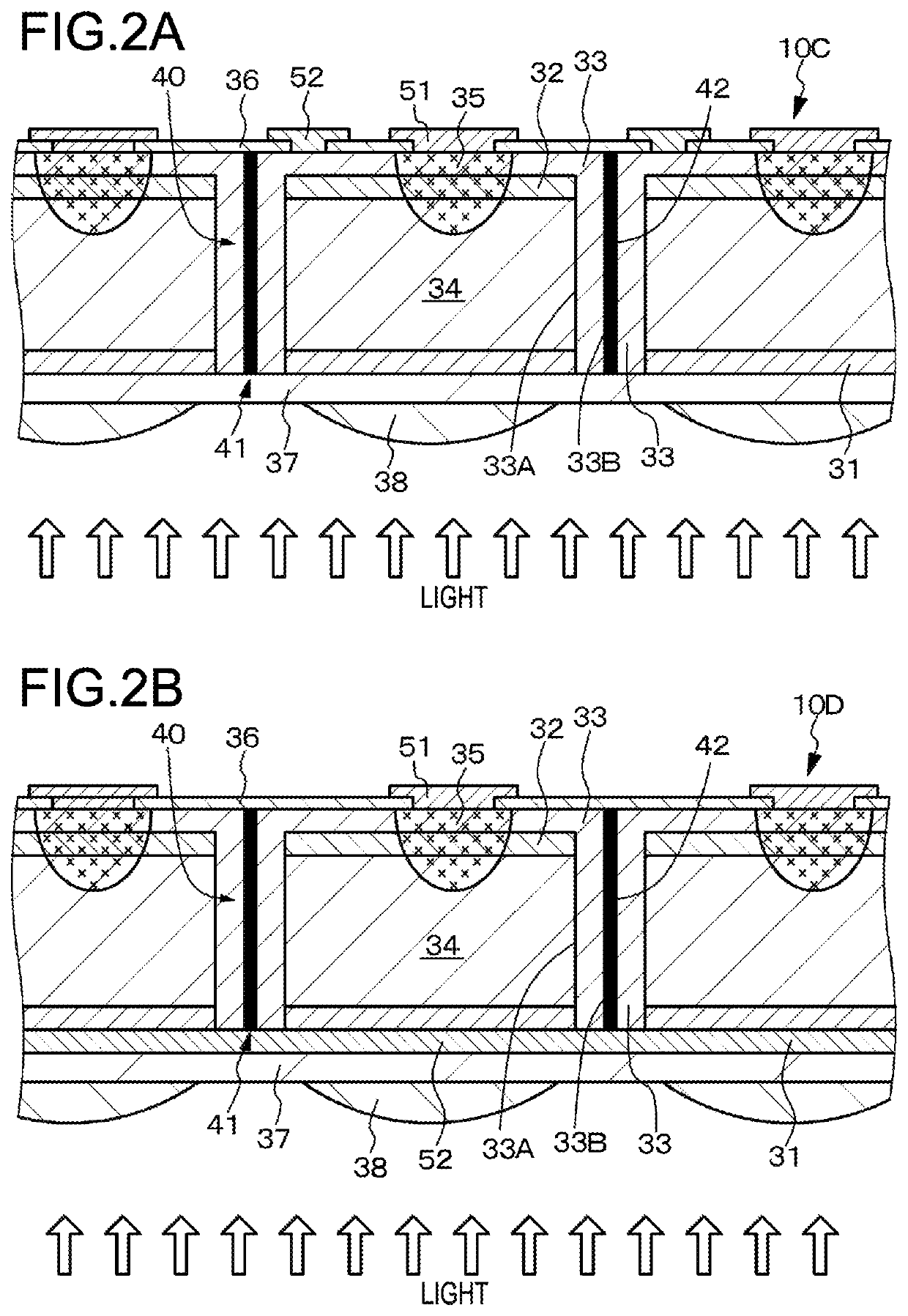
[0218]A second embodiment is a modification of the first embodiment. FIG. 2A shows a schematic partial cross-sectional view of the photoelectric conversion element of the second embodiment. FIG. 4B schematically shows the arrangement of a first electrode, a second electrode, a second compound semiconductor layer, an element isolation layer, a recess part, and a groove part in the photoelectric conversion element of the second embodiment.

[0219]In a photoelectric conversion element 10C of the second embodiment, a portion of an element isolation layer 33, which is held in contact with the lateral surface of a photoelectric conversion layer 34, is made of a third compound semiconductor material, and the other part of the element isolation layer 33 is made of an insulating material layer or a light shielding material layer 42. That is, a groove part 41 is formed in the portion of the element isolation layer 33 positioned inside a recess part 40 so as to surround the photoelectric convers...

third embodiment

[0224]A third embodiment is a modification of the photoelectric conversion elements of the first and second embodiments and relates to a method for manufacturing a photoelectric conversion element according to a second aspect of the present technology. Hereinafter, a description will be given of the method for manufacturing the photoelectric conversion element of the third embodiment with reference to FIGS. 16A, 16B, 16C, 17A, and 17B each showing a schematic partial end view of a first compound semiconductor layer or the like.

[0225][Step 300]

[0226]On a substrate, a first compound semiconductor layer 31 made of a first compound semiconductor material having a first conductivity type and a photoelectric conversion layer 34 are sequentially formed. Specifically, an InP substrate (film forming substrate) 21 made of InP and having a buffer layer 22 having a thickness of 0.1 μm to 1 μm is prepared. Further, the first compound semiconductor layer 31 having a thickness of 0.1 μm to 1 μm an...


PUM

PropertyMeasurementUnit
band gap energyaaaaaaaaaa
thicknessaaaaaaaaaa

Abstract

A photoelectric conversion element includes: a first compound semiconductor layer 31 made of a first compound semiconductor material having a first conductivity type; a photoelectric conversion layer 34 formed on the first compound semiconductor layer 31; a second compound semiconductor layer 32 covering the photoelectric conversion layer 34 and made of a second compound semiconductor material having the first conductivity type; a second conductivity type region 35 formed at least in a part of the second compound semiconductor layer 32, having a second conductivity type different from the first conductivity type, and reaching the photoelectric conversion layer; an element isolation layer 34 surrounding a lateral surface of the photoelectric conversion layer; a first electrode 51 formed on the second conductivity type region; and a second electrode 52 electrically connected to the first compound semiconductor layer 31.

Description

CROSS REFERENCE TO RELATED APPLICATIONS[0001]This application is a national stage application under 35 U.S.C. 371 and claims the benefit of PCT Application No. PCT / JP2017 / 004578 having an international filing date of 8 Feb. 2017, which designated the United States, which PCT application claimed the benefit of Japanese Patent Application No. 2016-051950 filed 16 Mar. 2016, and Japanese Patent Application No. 2016-189568 filed 28 Sep. 2016, the entire disclosures of each of which are incorporated herein by reference.TECHNICAL FIELD[0002]The present technology relates to a photoelectric conversion element, a method for manufacturing the same, and an imaging apparatus.BACKGROUND ART[0003]In general, an imaging apparatus includes photoelectric conversion elements (light-receiving elements, photodiodes, or imaging elements) formed on a silicon semiconductor substrate. Meanwhile, the light absorption coefficient of silicon (Si) is uniquely determined when the wavelength of incident light i...

Claims


Application Information

Patent Timeline
Patent Type & Authority Patents(United States)
IPC IPC(8): H01L31/0304H01L27/146H01L31/109H04N5/374H04N5/378H01L31/0216H01L31/0224H01L31/18H01L51/42
CPCH01L31/022408H01L27/14623H01L31/109H01L27/14645H01L31/1844H01L27/1463H01L31/03046H01L31/0304H01L31/1884H01L27/14689H01L27/14694H01L27/14621H04N5/378H01L31/02164H01L27/14649H04N5/374H01L31/022466H01L51/4253H01L27/14627Y02E10/544Y02P70/50H04N25/75H04N25/76H10K30/30
Inventor MANDA, SHUJIOKUYAMA, ATSUSHIMATSUMOTO, RYOSUKE
Owner SONY CORP
Why Eureka
Try Eureka