Etching method

a silicon oxide film and etching technology, applied in the direction of basic electric elements, semiconductor/solid-state device manufacturing, electric devices, etc., can solve the problems of insufficient improvement of the etching profile of silicon oxide films, inability to fill defects, and likely gaps (voids) in silicon oxide films, etc., to achieve the effect of improving the etching profile of silicon-containing oxide films

Active Publication Date: 2020-05-12
TOKYO ELECTRON LTD
View PDF10 Cites 0 Cited by
  • Summary
  • Abstract
  • Description
  • Claims
  • Application Information

AI Technical Summary

Benefits of technology

[0007]In one aspect, the present invention aims at improving an etching profile of silicon-containing oxide film by dry etching.

Problems solved by technology

If the etching pattern has such etching profile, in a post-process in which the etching pattern is filled with metal, a filling defect, in which a gap (void) is generated, is likely to occur.
However, in the method disclosed in Patent Document 1, because the side wall of the contact hole is wet etched by hydrofluoric acid after the mask on the silicon oxide film is removed by ashing using oxygen gas plasma, an etching profile of the silicon oxide film is not sufficiently improved.

Method used


Image

  • Etching method
  • Etching method
  • Etching method

Examples


Embodiment Construction

[0014]In the following, embodiments of the present invention will be described with reference to the drawings. Note that in the following descriptions and the drawings, elements having substantially identical features are given the same reference symbols and overlapping descriptions may be omitted.

[0015][Plasma Processing Apparatus]

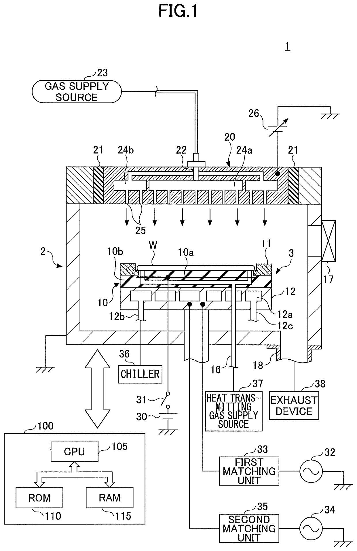
[0016]First, an example of a plasma processing apparatus 1 will be described with reference to FIG. 1. The plasma processing apparatus 1 according to a present embodiment is a capacitively coupled plasma type parallel-flat plate plasma processing apparatus, and includes a substantially cylindrical processing vessel (chamber) 2. To an internal surface of the processing vessel 2, anodic oxidation treatment is applied. An inside of the processing vessel 2 is a processing chamber for performing plasma treatment such as etching or depositing.

[0017]A stage 3 is used for placing a semiconductor wafer (hereinafter, it will be referred to as a “wafer”) which is an...


PUM

PropertyMeasurementUnit
pressureaaaaaaaaaa
frequencyaaaaaaaaaa
frequencyaaaaaaaaaa

Abstract

An etching method of silicon-containing oxide film is provided. The etching method includes a first step of forming an etching pattern on the silicon-containing oxide film by etching the silicon-containing oxide film using a first plasma generated from a first gas supplied to the processing vessel, according to a pattern of a mask layered on the silicon-containing oxide film, and a second step of removing a reaction product adhering to vicinity of an opening of the etching pattern and to the mask using a second plasma generated from a second gas supplied to the processing vessel, by applying a first high frequency electric power for generating plasma and a second high frequency electric power for generating bias voltage.

Description

CROSS-REFERENCE TO RELATED APPLICATIONS[0001]This patent application is based upon and claims the benefit of priority of Japanese Patent Application No. 2017-121596 filed on Jun. 21, 2017, the entire contents of which are incorporated herein by reference.BACKGROUND OF THE INVENTION1. Field of the Invention[0002]The present invention generally relates to an etching method.2. Description of the Related Art[0003]When silicon oxide film is etched by plasma in a pattern of a mask on the silicon oxide film, a reaction product adheres to vicinity of an opening of the silicon oxide film or an upper surface of the mask. If the reaction product adheres, after the mask is removed from the silicon oxide film by ashing, which is performed after etching, an etching profile of the silicon oxide tends to be of an inverted tapered shape, in which a side wall of an etching pattern formed in the silicon oxide film is not vertical and in which a width of the etching pattern at a bottom side is wider th...

Claims


Application Information

Patent Timeline
Patent Type & Authority Patents(United States)
IPC IPC(8): H01L21/768H01L21/02H01L21/311
CPCH01L21/02063H01L21/76879H01L21/31144H01L21/31116H01L21/76804H01L21/31138H01L21/3065H01L21/32136
Inventor MIZUNO, HIDEKI
Owner TOKYO ELECTRON LTD
Why Eureka
Try Eureka