

Interconnection structure and method of forming the same
a technology of interconnection structure and interconnection structure, which is applied in the direction of semiconductor devices, semiconductor/solid-state device details, electrical apparatus, etc., can solve the problems of increasing problems and limited speed at which future circuits will operate, and achieve the effects of reducing the overall dielectric constant, and reducing the interference of coupling between adjacent conductive structures
- Summary
- Abstract
- Description
- Claims
- Application Information
AI Technical Summary
Benefits of technology
Problems solved by technology
Method used
Image

Examples
first embodiment
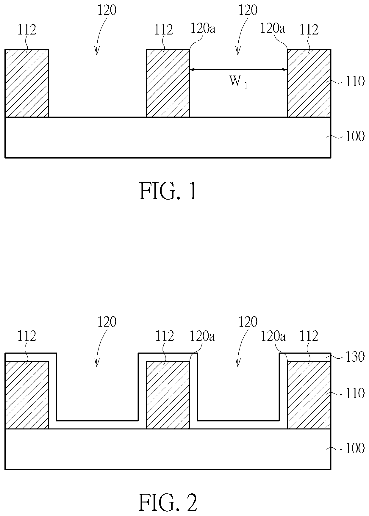
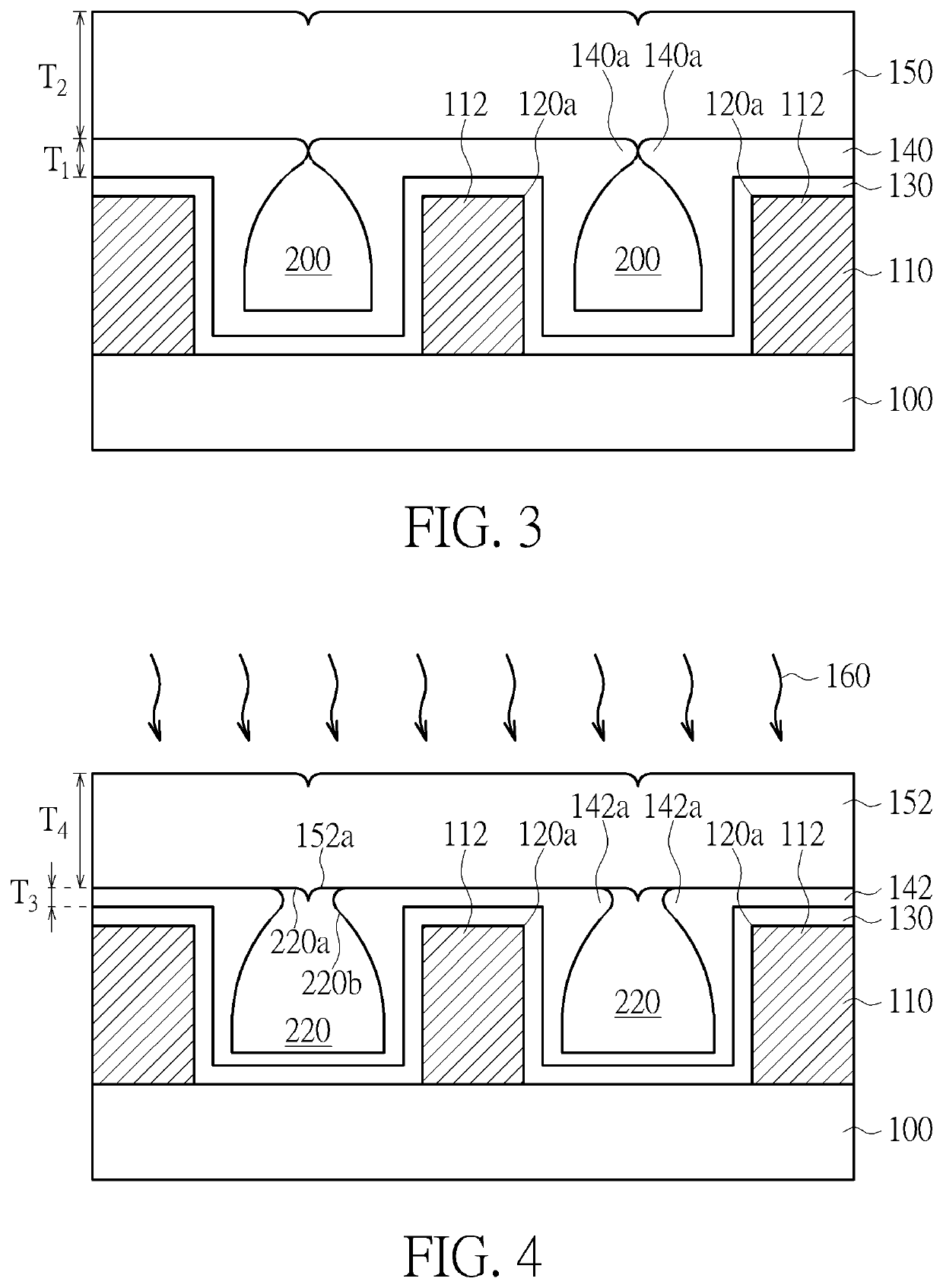
[0017]Please refer to FIG. 1 to FIG. 4, which are schematic diagrams illustrating the method for forming an interconnection structure according to the present invention. As shown in FIG. 1, a substrate 100 is provided. The substrate 100 could be a semiconductor substrate such as a silicon substrate, an epitaxial substrate, a silicon carbide (SiC) substrate, a silicon-on-insulator (SOI) substrate, but not limited thereto. The substrate 100 may be a semi-fabricated substrate for forming an integrated circuits device. The substrate 100 may have semiconductor devices formed therein, such as metal-oxide semiconductor (MOS) transistors, diodes, bipolar junction transistors (BJTs), capacitors or other integrated circuit components. The substrate 100 may also have multiple material layers such as interlayer or intermetal dielectric layers and interconnection structures such as metal lines or vias formed therein. A patterned layer 110 is formed on the substrate 100. The patterned layer 110 m...
second embodiment
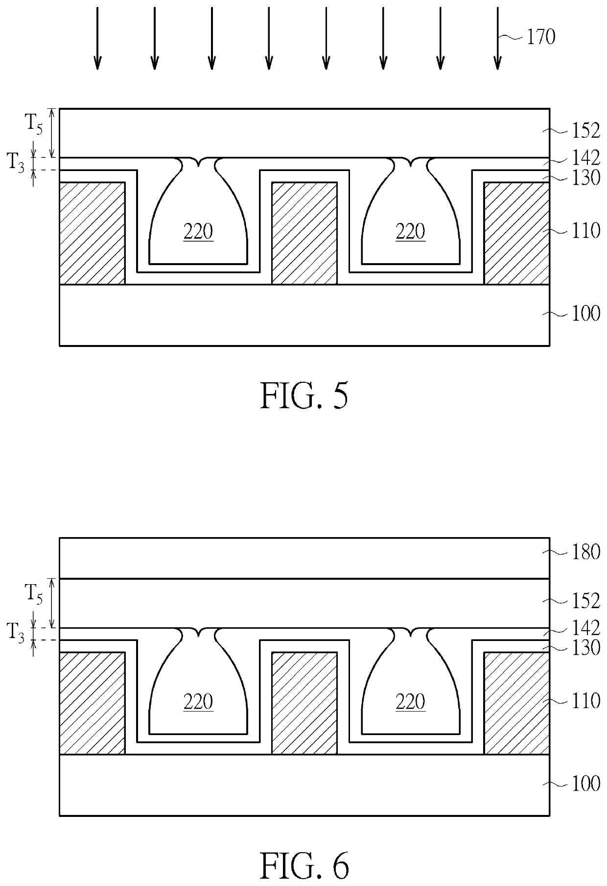
[0027]Please refer to FIG. 6, which is a schematic diagram illustrating the present invention. Optionally, a third dielectric layer 180 may be formed on the second dielectric layer 152 after the curing process 160. The third dielectric layer 180 may be a low-k dielectric material including carbon-doped silicon dioxide materials, fluorinated silicate glass (FSG), organic polymeric thermoset materials, silicon oxycarbide, SiCOH dielectrics, fluorine doped silicon oxide, spin-on glasses, benzocyclobutene (BCB)-based polymer dielectrics, silsesquioxanes including hydrogen silsesquioxane (HSQ), methyl silsesquioxane (MSQ) and mixtures or copolymers of HSQ and MSQ, but not limited thereto. The third dielectric layer 180 may be formed on the second dielectric layer 152 after the planarization process 170. In other embodiments, the third dielectric layer 180 may be formed on the second dielectric layer 152 after the curing process 160 and then be planarized.
[0028]Please refer to FIG. 7, whi...
PUM
| Property | Measurement | Unit |
|---|---|---|
| dielectric constant | aaaaa | aaaaa |
| width W1 | aaaaa | aaaaa |
| thickness T1 | aaaaa | aaaaa |
Abstract
Description
Claims
Application Information