Semiconductor apparatus

a technology of semiconductor apparatus and semiconductor atomizer, which is applied in the direction of electrical apparatus, semiconductor device details, semiconductor/solid-state device devices, etc., can solve the problems of short life of the overall semiconductor apparatus, inability to uniformize the temperature of the unit transistor, and reduce the radio-frequency characteristics of the semiconductor apparatus. , to achieve the effect of reducing the temperature difference and reducing the non-uniform temperatur

Active Publication Date: 2020-08-04
MURATA MFG CO LTD
View PDF5 Cites 0 Cited by
  • Summary
  • Abstract
  • Description
  • Claims
  • Application Information

AI Technical Summary

Benefits of technology

[0007]It is an object of the present disclosure to provide a semiconductor apparatus that is capable of fulfilling the performance of the overall transistor by reducing the temperature variations during the operation of plural unit transistors formed on a substrate where an operating current flows.
[0011]The heat generated in the operating regions or the effective operating regions are conducted to the top surface of the metal member via the metal member disposed within the cavity. If the position of the cavity is displaced from that of the operating region or if the area of the overlapping region is differentiated among the effective operating regions, the heat dissipation becomes different among the operating regions or the effective operating regions. Hence, when the temperatures of the operating regions or the effective operating regions are non-uniform, varying of the heat dissipation among the operating regions or the effective operating regions to reduce the non-uniformity of the temperatures can reduce the temperature difference among the operating regions or the effective operating regions.

Problems solved by technology

When operating the parallel-connected plural unit transistors, the temperatures of the unit transistors may not become uniform.
A unit transistor where the temperature is likely to rise is degraded more quickly than the other unit transistors, and the life of the overall semiconductor apparatus becomes short.
Such temperature variations also decrease the radio-frequency characteristics of the semiconductor apparatus.

Method used


Image

  • Semiconductor apparatus
  • Semiconductor apparatus
  • Semiconductor apparatus

Examples


first embodiment

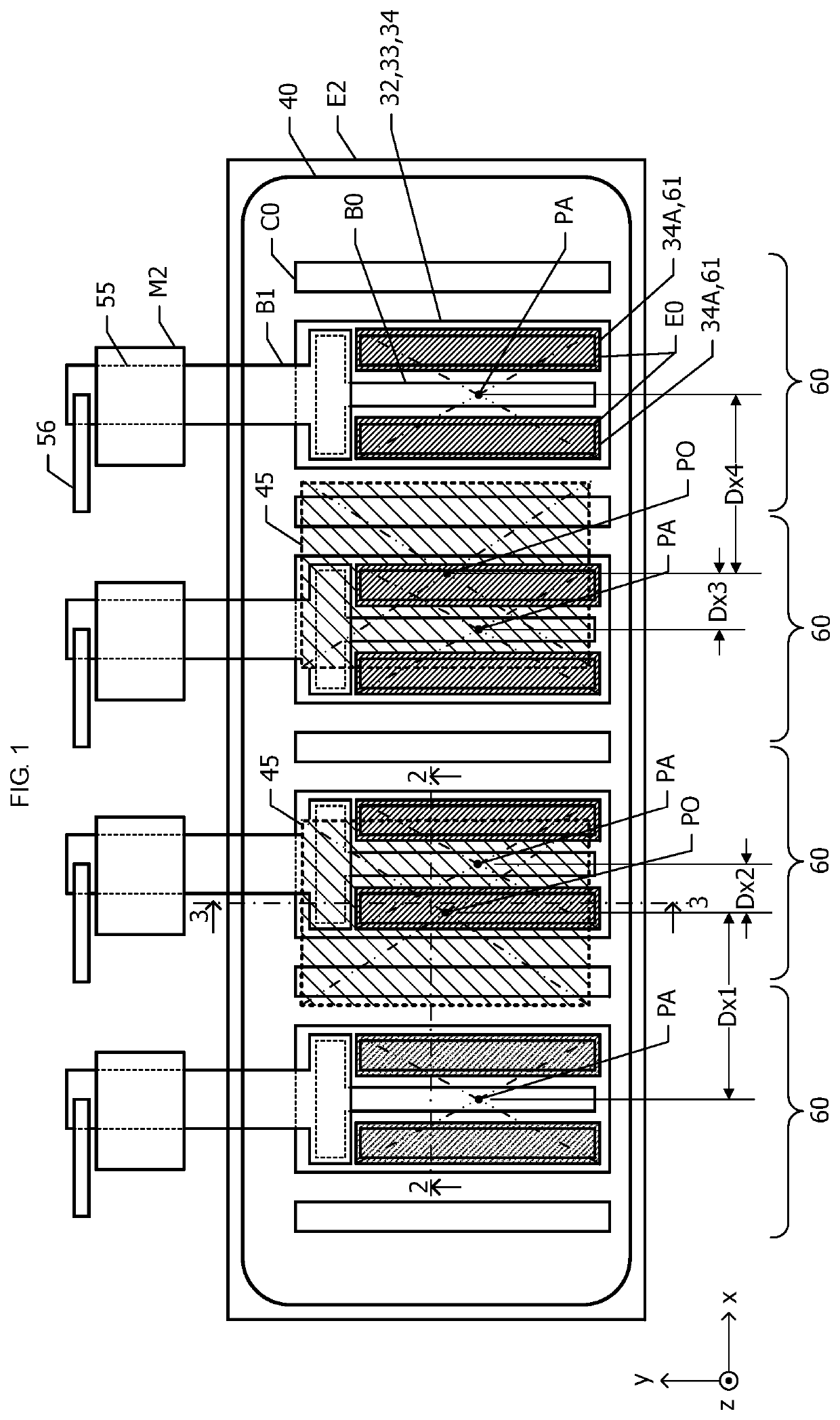
[0048]A semiconductor apparatus according to a first embodiment will be described below with reference to FIGS. 1 through 5B.

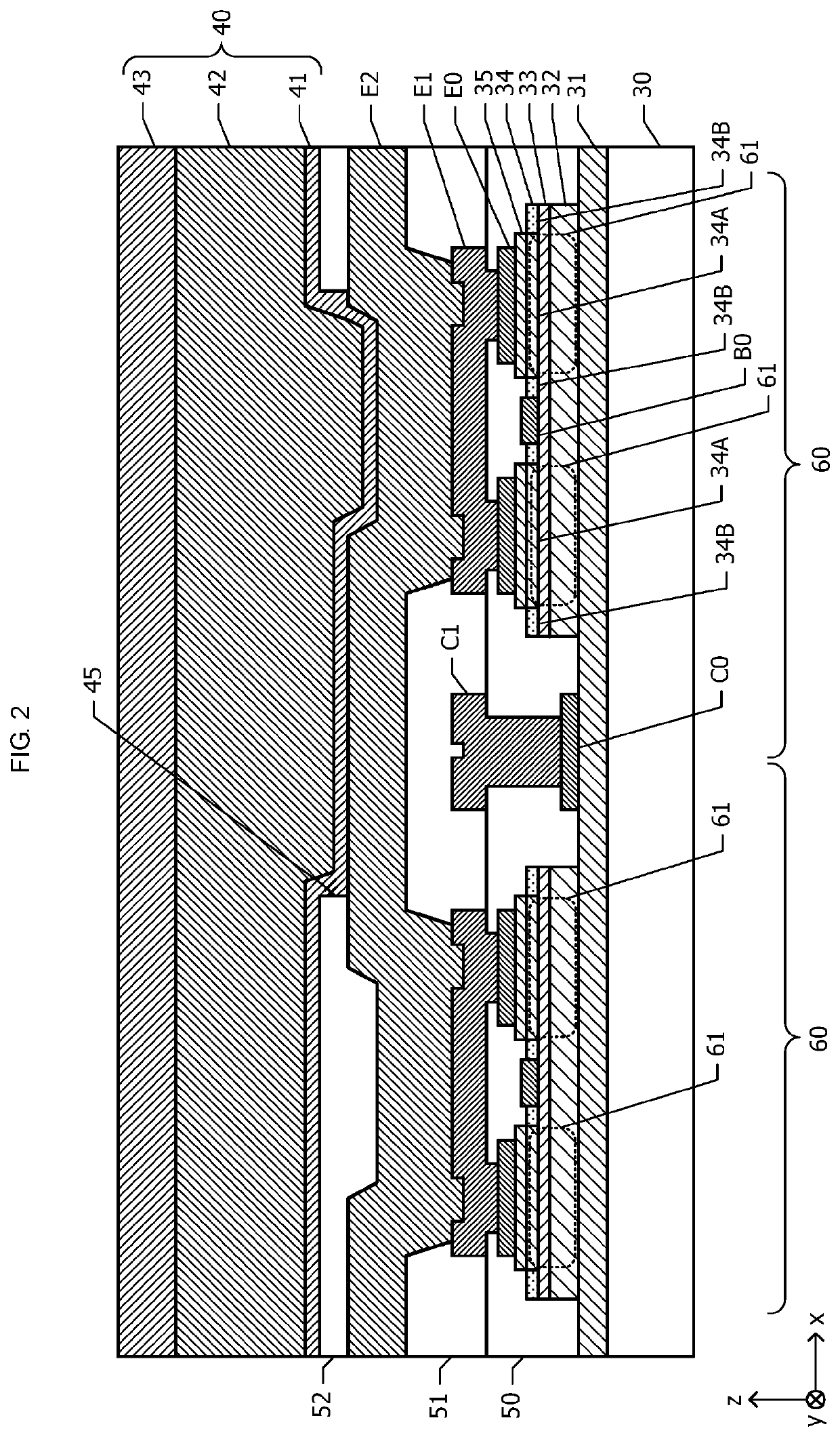
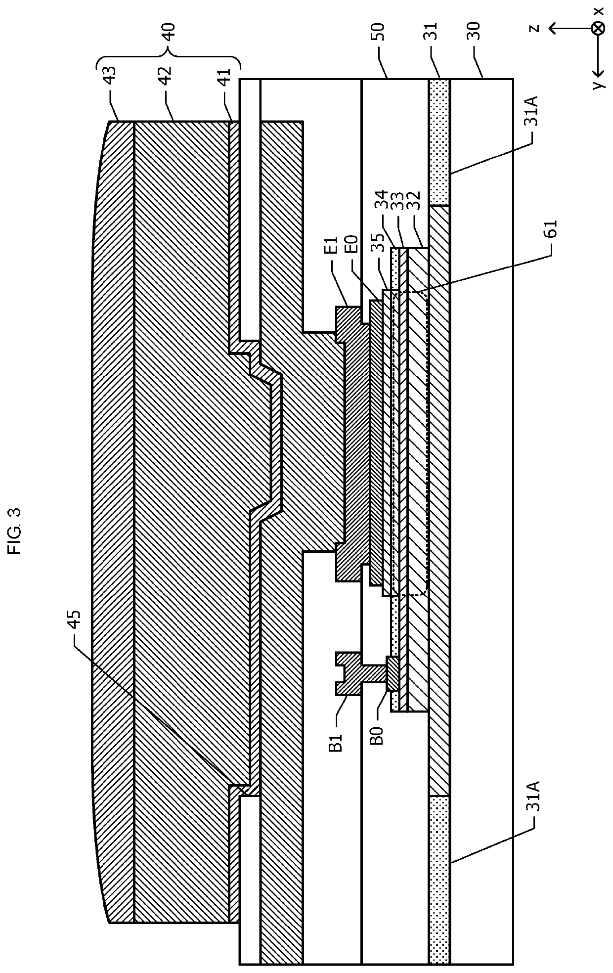
[0049]FIG. 1 is a plan view illustrating the layout of the elements forming the semiconductor apparatus according to the first embodiment. FIG. 2 is a sectional view taken along the long-dashed dotted line 2-2 in FIG. 1. FIG. 3 is a sectional view taken along the long-dashed dotted line 3-3 in FIG. 1. The semiconductor apparatus is constituted by plural elements stacked on each other. To make it easy to differentiate the elements of the semiconductor apparatus, some elements located on the lower side and hidden under the elements on the upper side are indicated by the broken lines, though they are not actually seen from above in FIG. 1. The outer edges of some elements are indicated by the broken lines, and some elements are indicated by the hatched portions with different densities.

[0050]In the drawings, an xyz rectangular coordinate system is defined. In thi...

second embodiment

[0106]A semiconductor apparatus according to a second embodiment will be described below with reference to FIG. 6. An explanation of the elements configured in the same manner as those of the first embodiment will be omitted.

[0107]FIG. 6 is a plan view illustrating the layout of the elements forming the semiconductor apparatus according to the second embodiment. In the second embodiment, three unit transistors 60 are arranged in the x-axis direction. However, four unit transistors 60 may be provided, as in the first embodiment, or two or five or more unit transistors 60 may be provided. In the first embodiment, one unit transistor 60 includes two emitter regions 34A (FIGS. 1 and 2). In the second embodiment, one unit transistor 60 includes one emitter region 34A, that is, one unit transistor 60 includes one operating region 61. The operating region 61 is defined by the outer edge lines of the emitter region 34A for each unit transistor 60. In FIG. 6, the operating regions 61 are ind...

third embodiment

[0111]A semiconductor apparatus according to a third embodiment will be described below with reference to FIGS. 7 through 11. An explanation of the elements configured in the same manner as those of the first embodiment will be omitted. The semiconductor apparatus of the third embodiment is a power amplifier module using the plural unit transistors 60 (FIG. 1) of the first embodiment as amplifiers.

[0112]FIG. 7 is an equivalent circuit diagram of a power amplifier circuit implemented by the semiconductor apparatus according to the third embodiment. The power amplifier circuit in the third embodiment amplifies an input signal in a radio-frequency band and outputs an amplified signal. The frequency of the input signal is in a range of several hundreds of megahertz (about 600 MHz, for example) to several dozens of gigahertz (60 GHz, for example).

[0113]The power amplifier circuit using the semiconductor apparatus according to the third embodiment includes transistors Q1 and Q2, matching ...


PUM

PropertyMeasurementUnit
currentaaaaaaaaaa
widthaaaaaaaaaa
widthaaaaaaaaaa

Abstract

A wiring is disposed above operating regions of plural unit transistors arranged on a substrate in a first direction. An insulating film is disposed on the wiring. A cavity entirely overlapping with the wiring as viewed from above is formed in the insulating film. A metal member electrically connected to the wiring via the cavity is disposed on the insulating film. The centroid of the cavity is displaced from that of the operating region of the corresponding unit transistor in the first direction. When the cavity having a centroid the closest to the operating region of a unit transistor is defined as the closest proximity cavity, the amount of deviation of the centroid of the closest proximity cavity from that of the operating region of the corresponding unit transistor in the first direction becomes greater from the center to the ends of the arrangement direction of the unit transistors.

Description

[0001]This application claims priority from Japanese Patent Application No. 2017-234278, filed on Dec. 6, 2017, Japanese Patent Application No. 2018-115799, filed on Jun. 19, 2018, and Japanese Patent Application No. 2018-168440, filed on Sep. 10, 2018. The content of these applications are incorporated herein by reference in their entireties.BACKGROUND OF THE DISCLOSURE1. Field of the Disclosure[0002]The present disclosure relates to a semiconductor apparatus.2. Description of the Related Art[0003]A heterojunction bipolar transistor (HBT) is used for a power amplifier module of, for example, a mobile terminal. In the semiconductor apparatus disclosed in Japanese Unexamined Patent Application Publication No. 2003-77930, a bump is disposed immediately above an HBT. The bump is electrically connected to the HBT via a cavity formed in an insulating film disposed between the HBT and the bump. The entirety of the HBT is disposed within the cavity. With this configuration, the distance fr...

Claims


Application Information

Patent Timeline
Patent Type & Authority Patents(United States)
IPC IPC(8): H01L23/49H01L23/528H01L23/532H01L23/29H01L23/14H01L23/00
CPCH01L23/49H01L23/296H01L23/147H01L23/53228H01L23/528H01L2224/32225H01L2224/0346H01L2224/13083H01L2224/92244H01L24/73H01L2924/19042H01L24/92H01L24/05H01L2224/13147H01L2224/0401H01L2224/05569H01L2224/04105H01L2224/13111H01L2924/19105H01L2224/13155H01L2224/05572H01L2224/73267H01L2224/16227H01L24/16H01L2224/131H01L2924/19041H01L2224/12105H01L2224/13082H01L24/13H01L2224/05548H01L2224/05647H01L24/32H01L2924/013H01L2924/00014H01L23/3677H01L27/082
Inventor KUROKAWA, ATSUSHIAOIKE, MASAYUKITSUTSUI, TAKAYUKI
Owner MURATA MFG CO LTD
Why Eureka
Try Eureka