
Compound, resin, and purification method thereof, material for forming underlayer film for lithography, composition for forming underlayer film, and underlayer film, as well as resist pattern forming method and circuit pattern forming method

a technology of resist pattern forming and resin, which is applied in the field of compound, resin, and purification method, can solve the problems of high solvent solubility, and achieve the effect of excellent heat resistance and etching resistan

Active Publication Date: 2020-08-18
MITSUBISHI GAS CHEM CO INC
View PDF136 Cites 2 Cited by
  • Summary
  • Abstract
  • Description
  • Claims
  • Application Information

AI Technical Summary

Benefits of technology

The present invention aims to provide a compound that can be applied to a wet process and used to form a photoresist underlayer film that is resistant to heat and etching. This compound can serve as a material for lithography processes.

Problems solved by technology

As described above, many materials for forming an underlayer film for lithography have been conventionally proposed, but there are no ones that not only have such a high solvent solubility as to be able to be applied to a wet process such as a spin coating method or screen printing, but also simultaneously satisfy heat resistance and etching resistance at a high level, and thus a new material is required to be developed.

Method used


Image

  • Compound, resin, and purification method thereof, material for forming underlayer film for lithography, composition for forming underlayer film, and underlayer film, as well as resist pattern forming method and circuit pattern forming method
  • Compound, resin, and purification method thereof, material for forming underlayer film for lithography, composition for forming underlayer film, and underlayer film, as well as resist pattern forming method and circuit pattern forming method
  • Compound, resin, and purification method thereof, material for forming underlayer film for lithography, composition for forming underlayer film, and underlayer film, as well as resist pattern forming method and circuit pattern forming method

Examples


example 11

[0245]Then, the composition for forming an underlayer film for lithography in Example 6 was coated on a SiO2 substrate having a film thickness of 300 nm, and baked at 240° C. for 60 seconds and further at 400° C. for 120 seconds to thereby form an underlayer film having a film thickness of 85 nm. A resist solution for ArF was coated on the underlayer film, and baked at 130° C. for 60 seconds to thereby form a photoresist layer having a film thickness of 140 nm. Herein, as the resist solution for ArF, one prepared by blending 5 parts by mass of the compound of the following formula (3), 1 part by mass of triphenylsulfonium nonafluoromethanesulfonate, 2 parts by mass of tributylamine, and 92 parts by mass of PGMEA was used.

[0246]A compound of the following formula (3) was prepared as follows. That is, 4.15 g of 2-methyl-2-methacryloyloxyadamantane, 3.00 g of methacryloyloxy-γ-butyrolactone, 2.08 g of 3-hydroxy-1-adamantyl methacrylate and 0.38 g of azobisisobutyronitrile were dissolve...

example 12

[0254]The composition for forming an underlayer film for lithography used in Example 6 was coated on a SiO2 substrate having a film thickness of 300 nm, and baked at 240° C. for 60 seconds and further at 400° C. for 120 seconds to thereby form an underlayer film having a film thickness of 90 nm. A silicon-containing intermediate layer material was coated on the underlayer film, and baked at 200° C. for 60 seconds to thereby form an intermediate layer film having a film thickness of 35 nm. Furthermore, the resist solution for ArF was coated on the intermediate layer film, and baked at 130° C. for 60 seconds to thereby form a photoresist layer having a film thickness of 150 nm. Herein, a silicon atom-containing polymer obtained as described below was used as the silicon-containing intermediate layer material.

[0255]In 200 g of tetrahydrofuran (THF) and 100 g of pure water were dissolved 16.6 g of 3-carboxylpropyltrimethoxysilane, 7.9 g of phenyltrimethoxysilane and 14.4 g of 3-hydroxyp...

example 13

(Example 13) Purification of BiF-I-1

[0277]To a four-neck flask (bottom outlet type) having a volume of 1000 mL was charged 150 g of a solution (10% by mass) in which BiF-I-1 obtained in Example 1 was dissolved in PGMEA, and heated to 80° C. with stirring. Then, 37.5 g of an aqueous oxalic acid solution (pH: 1.3) was added thereto, stirred for 5 minutes and thereafter left to stand for 30 minutes. The resultant was thus separated to an oil phase and an aqueous phase, and therefore the aqueous phase was removed. Such an operation was repeated once, and thereafter the resulting oil phase was charged with 37.5 g of ultrapure water, stirred for 5 minutes and thereafter left to stand for 30 minutes to remove the aqueous phase. Such an operation was repeated three times, and thereafter the flask was subjected to pressure reduction to 200 hPa or less while being heated to 80° C., to thereby allow the remaining water content and PGMEA to be distilled off by concentration. Thereafter, dilutio...


PUM

PropertyMeasurementUnit
temperatureaaaaaaaaaa

Abstract

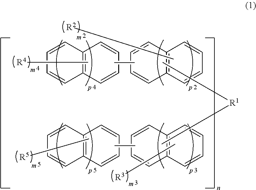
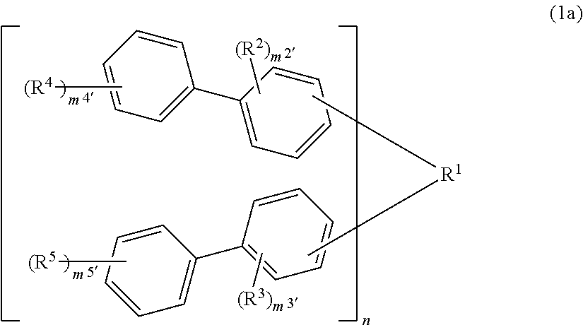
The present invention provides a compound represented by following formula (1),wherein R1 represents a 2n-valent group having 1 to 30 carbon atoms, each of R2 to R5 independently represents a straight, branched or cyclic alkyl group having 1 to 10 carbon atoms, an aryl group having 6 to 10 carbon atoms, an alkenyl group having 2 to 10 carbon atoms, an alkoxy group having 1 to 30 carbon atoms, a halogen atom, a thiol group or a hydroxyl group, provided that at least one selected from R1 to R5 represents a group including an iodine atom and at least one R4 and / or at least one R5 represent / represents one or more selected from the group consisting of a hydroxyl group and a thiol group, each of m2 and m3 independently represents an integer of 0 to 8, each of m4 and m5 independently represents an integer of 0 to 9, provided that m4 and m5 do not represent 0 at the same time, n represents an integer of 1 to 4, and each of p2 to p5 independently represents an integer of 0 to 2.

Description

CROSS-REFERENCE TO RELATED APPLICATIONS[0001]This application is a U.S. national phase application filed under 35 U.S.C. § 371 of International Application PCT / JP2016 / 058517, filed on Mar. 17, 2016, designating the United States, which claims priority from Japanese Application Number 2015-069989, filed Mar. 30, 2015, which are hereby incorporated herein by reference in their entirety.FIELD OF THE INVENTION[0002]The present invention relates to a compound, a resin, and a purification method thereof, a material for forming an underlayer film for lithography, a composition for forming an underlayer film, and an underlayer film, as well as a resist pattern forming method and a circuit pattern forming method.BACKGROUND OF THE INVENTION[0003]Semiconductor devices are manufactured through microfabrication by lithography using a photoresist material, but are required to be made finer by a pattern rule in accordance with the increase in integration degree and the increase in speed of LSI in ...

Claims


Application Information

Patent Timeline
Patent Type & Authority Patents(United States)
IPC IPC(8): G03F7/11H01L21/027C08F32/08C08G8/20C07C41/38C07C37/72G03F7/038C07C39/367C07C43/23C08G8/14C08K5/00C08K5/07C08K5/09
CPCC08F32/08C07C37/72H01L21/027G03F7/11C07C43/23C08G8/20C07C39/367G03F7/0382C08G8/14C07C41/38C08K5/07C08K5/09C08K5/0025C08L2203/16C07C39/15H01L21/0273H01L21/31144
Inventor TOIDA, TAKUMIECHIGO, MASATOSHIMAKINOSHIMA, TAKASHI
Owner MITSUBISHI GAS CHEM CO INC
Learn More