Using stochastic failure metrics in semiconductor manufacturing

a technology of failure metrics and stochastic failure, applied in semiconductor/solid-state device testing/measurement, image enhancement, instruments, etc., can solve problems such as the inability to perform defect classification based on the classification of defects, the inability to detect defects of decreasing size, and the difficulty in detecting defects

Active Publication Date: 2020-10-27
KLA CORP
View PDF18 Cites 8 Cited by
  • Summary
  • Abstract
  • Description
  • Claims
  • Application Information

AI Technical Summary

Problems solved by technology

However, as the dimensions of semiconductor devices decrease, inspection becomes even more important to the successful manufacture of acceptable semiconductor devices because smaller defects can cause the devices to fail.
For instance, as the dimensions of semiconductor devices decrease, detection of defects of decreasing size has become necessary because even relatively small defects may cause unwanted aberrations in the semiconductor devices.
Defect classification often cannot be performed based on just images or information generated by a wafer inspection tool.
The effects of PSN are particularly problematic for EUV with the lower number of photons associated with these lithographic processes.
As a result, certain fabrication defects may occur stochastically, even under nominally identical fabrication conditions.
Stochastic defects are becoming a problem for advanced design rules.
Stochastically-occurring fabrication defects, or stochastic defects, may occur with a certain probability when nominally identical structures are fabricated under nominally identical conditions at multiple locations within a field, at a given location across multiple fields on a single wafer, or at a given location on a sample across multiple wafers.
Stochastic defects may present multiple challenges in a fabrication environment.
Typically, defects may be assumed to be deterministic such that a known defect will consistently be present when fabricated according to a known production recipe including a pattern of elements to be fabricated on a sample and exposure parameters.
Accordingly, the presence of stochastic defects that do not always occur under given exposure conditions may introduce uncertainty into typical PWQ algorithms.
These previous techniques are not able to cover larger wafer area, can only cover limited number of critical features, and do not use a direct output of inspection system or yield management software.
SEM image based offline analysis typically also cannot cover a high number of critical features in timely manner.
Previous techniques also did not consider design when determining stochastic failures.

Method used


Image

  • Using stochastic failure metrics in semiconductor manufacturing
  • Using stochastic failure metrics in semiconductor manufacturing
  • Using stochastic failure metrics in semiconductor manufacturing

Examples


Embodiment Construction

[0035]Although claimed subject matter will be described in terms of certain embodiments, other embodiments, including embodiments that do not provide all of the benefits and features set forth herein, are also within the scope of this disclosure. Various structural, logical, process step, and electronic changes may be made without departing from the scope of the disclosure. Accordingly, the scope of the disclosure is defined only by reference to the appended claims.

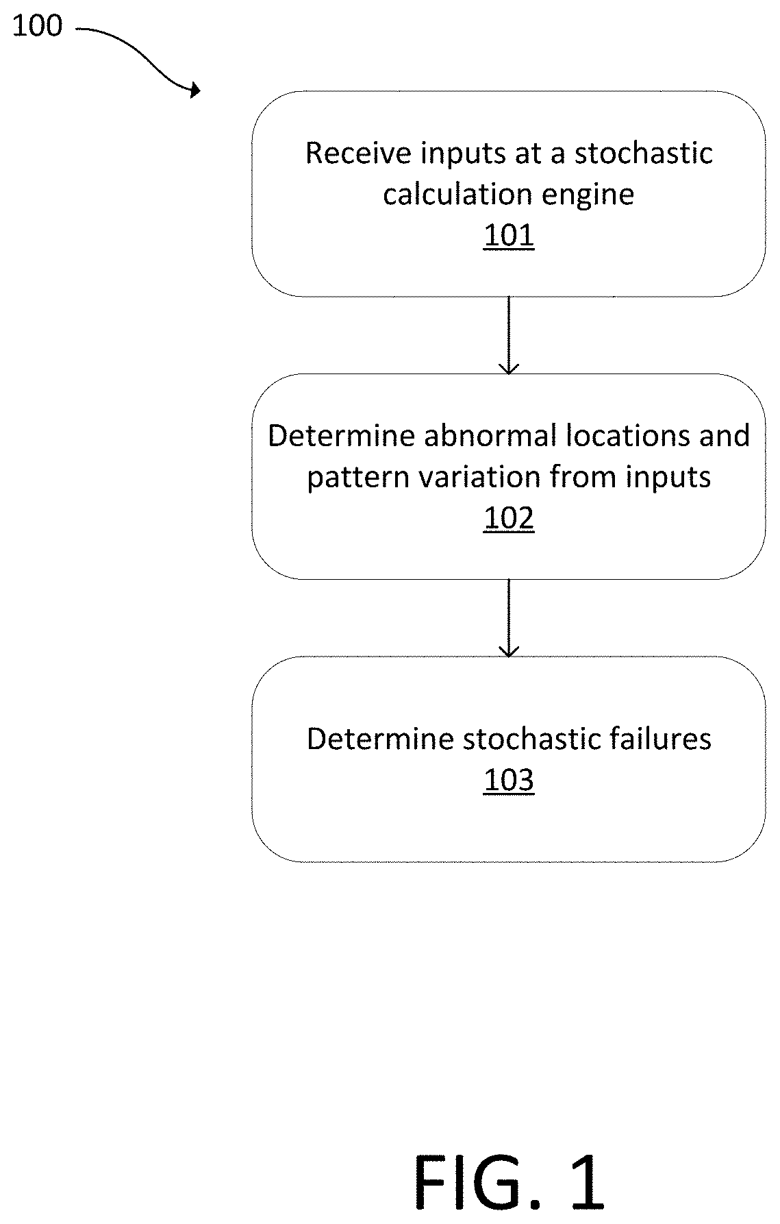
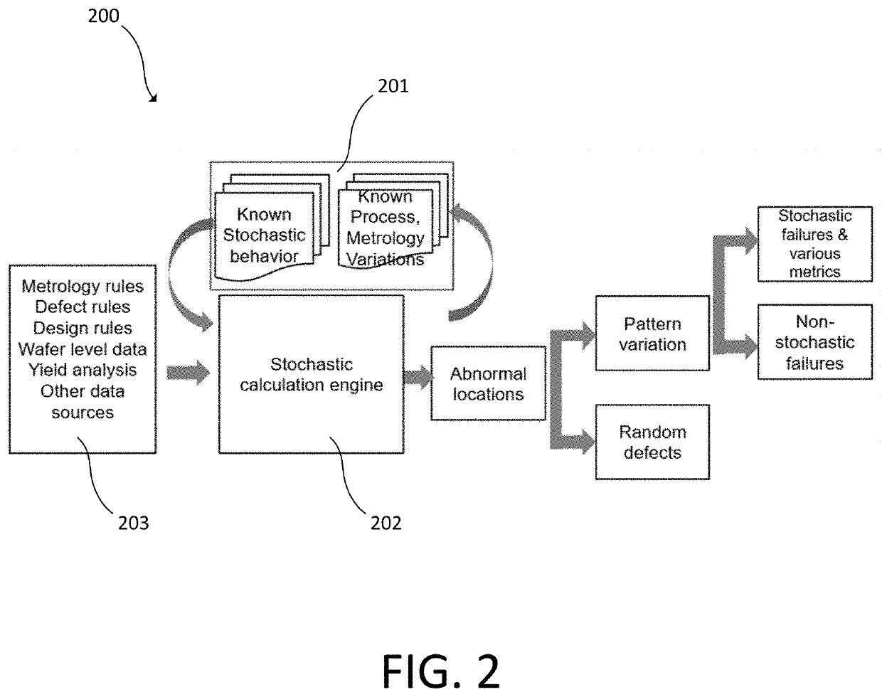
[0036]Embodiments disclosed herein use an integrated circuit (IC) design file to guide inspection. The IC design file can be used to conduct analysis of optical and / or electron beam inspection to output a stochastic failure metric for a semiconductor fabrication process. The IC design file also can be used to provide a direct output from an inspection system or yield management software.

[0037]To obtain reasonable stochastic failure rate of a given feature with statistical significance, large area inspections are generally...


PUM

PropertyMeasurementUnit
defectsaaaaaaaaaa
total timeaaaaaaaaaa
sizeaaaaaaaaaa

Abstract

A stochastic calculation engine receives inputs from a semiconductor inspection tool or semiconductor review tool. The stochastic calculation engine determines abnormal locations and pattern variation from the inputs and determines stochastic failures from the inputs. An electronic data storage unit connected with the stochastic calculation engine can include a database with known stochastic behavior and known process metrology variations. The stochastic calculation engine can flag stochastic features, determine a failure rate, or determine fail probability.

Description

CROSS-REFERENCE TO RELATED APPLICATIONS[0001]This application claims priority to the provisional patent application filed Sep. 7, 2018 and assigned U.S. App. No. 62 / 728,708, the disclosure of which is hereby incorporated by reference.FIELD OF THE DISCLOSURE[0002]This disclosure relates to semiconductor inspection and metrology.BACKGROUND OF THE DISCLOSURE[0003]Evolution of the semiconductor manufacturing industry is placing greater demands on yield management and, in particular, on metrology and inspection systems. Critical dimensions continue to shrink, yet the industry needs to decrease time for achieving high-yield, high-value production. Minimizing the total time from detecting a yield problem to fixing it determines the return-on-investment for a semiconductor manufacturer.[0004]Fabricating semiconductor devices, such as logic and memory devices, typically includes processing a semiconductor wafer using a large number of fabrication processes to form various features and multip...

Claims


Application Information

Patent Timeline
Patent Type & Authority Patents(United States)
IPC IPC(8): G06T7/00G01N21/95
CPCG06T7/0004G01N21/9501G06T2207/30148G06T2207/10061G06T2207/20084H01L22/20H01L22/12H01L21/67242H01L22/30H01L22/26H01L22/22H01L22/10
Inventor LEUNG, WING-SHAN RIBISAH, KAUSHIKPARK, ALLENCROSS, ANDREW
Owner KLA CORP
Why Eureka
Try Eureka