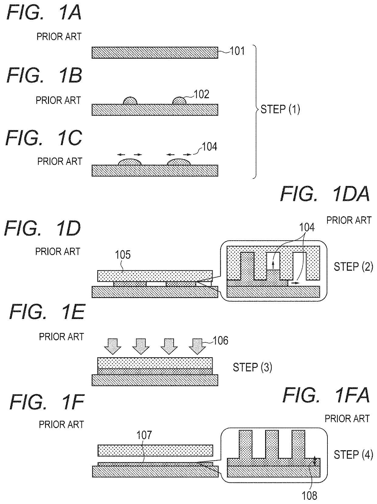
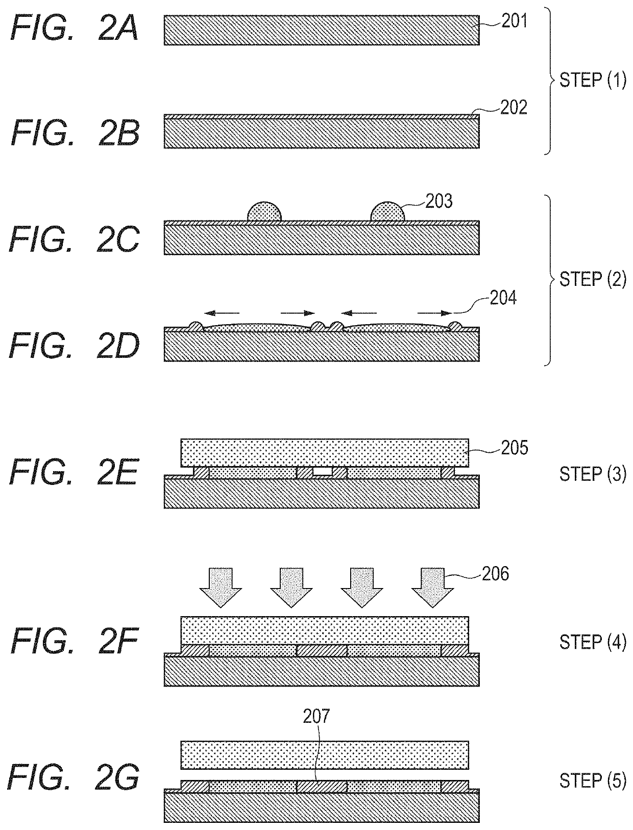
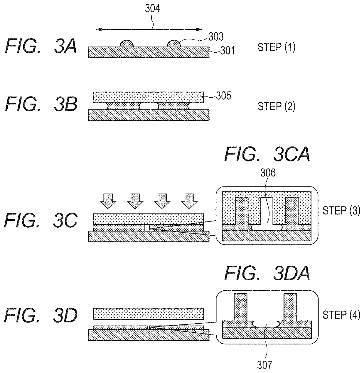
Pattern forming method as well as production methods for processed substrate, optical component, circuit board, electronic component and imprint mold
a technology of substrate and forming method, applied in the direction of instruments, photomechanical devices, inks, etc., can solve the problem of low throughput and achieve the effect of reducing productivity, high throughput and high throughpu
- Summary
- Abstract
- Description
- Claims
- Application Information
AI Technical Summary
Benefits of technology
Problems solved by technology
Method used
Image

Examples
example 1
[0176](1) Preparation of Curable Composition (A1-1)
[0177]As shown in Table 1, 50 parts by weight of neopentyl glycol diacrylate serving as the component (a1), 33,000 parts by weight of propylene glycol monomethyl ether acetate serving as the component (d1), and 50 parts by weight of pentaerythritol tetrakis(3-mercaptobutyrate) serving as the component (e1) were blended, and the blend was filtered with a 0.2-micrometer filter made of an ultrahigh-molecular weight polyethylene to prepare a curable composition (A1-1).
[0178](2) Measurement of Surface Tension of Curable Composition (A1-1)
[0179]The surface tension of a composition of the components of the curable composition (A1-1) except the component (d1) serving as a solvent at 25° C. was measured with an automatic surface tension meter DY-300 (manufactured by Kyowa Interface Science Co., Ltd.) by a plate method involving using a platinum plate. As a result, the surface tension was 33.7 mN / m. The measurement was performed under the con...
PUM
| Property | Measurement | Unit |
|---|---|---|
| wt % | aaaaa | aaaaa |
| boiling point | aaaaa | aaaaa |
| boiling point | aaaaa | aaaaa |
Abstract
Description
Claims
Application Information
 - R&D
- Intellectual Property
- Life Sciences
- Materials
- Tech Scout
- Unparalleled Data Quality
- Higher Quality Content
- 60% Fewer Hallucinations
Browse by: Latest US Patents, China's latest patents, Technical Efficacy Thesaurus, Application Domain, Technology Topic, Popular Technical Reports.
© 2025 PatSnap. All rights reserved.Legal|Privacy policy|Modern Slavery Act Transparency Statement|Sitemap|About US| Contact US: help@patsnap.com