
Supply voltage and temperature independent receiver

Active Publication Date: 2020-12-15
APPLE INC
View PDF6 Cites 0 Cited by
  • Summary
  • Abstract
  • Description
  • Claims
  • Application Information

AI Technical Summary

Benefits of technology

The patent is about a circuit that includes two inverter circuits that work together to control the voltage signal between two nodes. The first inverter has a certain threshold voltage, while the second inverter has a lower threshold voltage. The circuit includes specific types of transistors that form the core of each inverter circuit. The technical effect of this invention is to provide a more efficient and effective control of voltage signals in a circuit.

Problems solved by technology

However, operation of the conventional CMOS based inverter circuit is typically dependent on temperature as well as voltage supply ripples and other variations.

Method used


Image

  • Supply voltage and temperature independent receiver
  • Supply voltage and temperature independent receiver
  • Supply voltage and temperature independent receiver

Examples


example electronic

Device

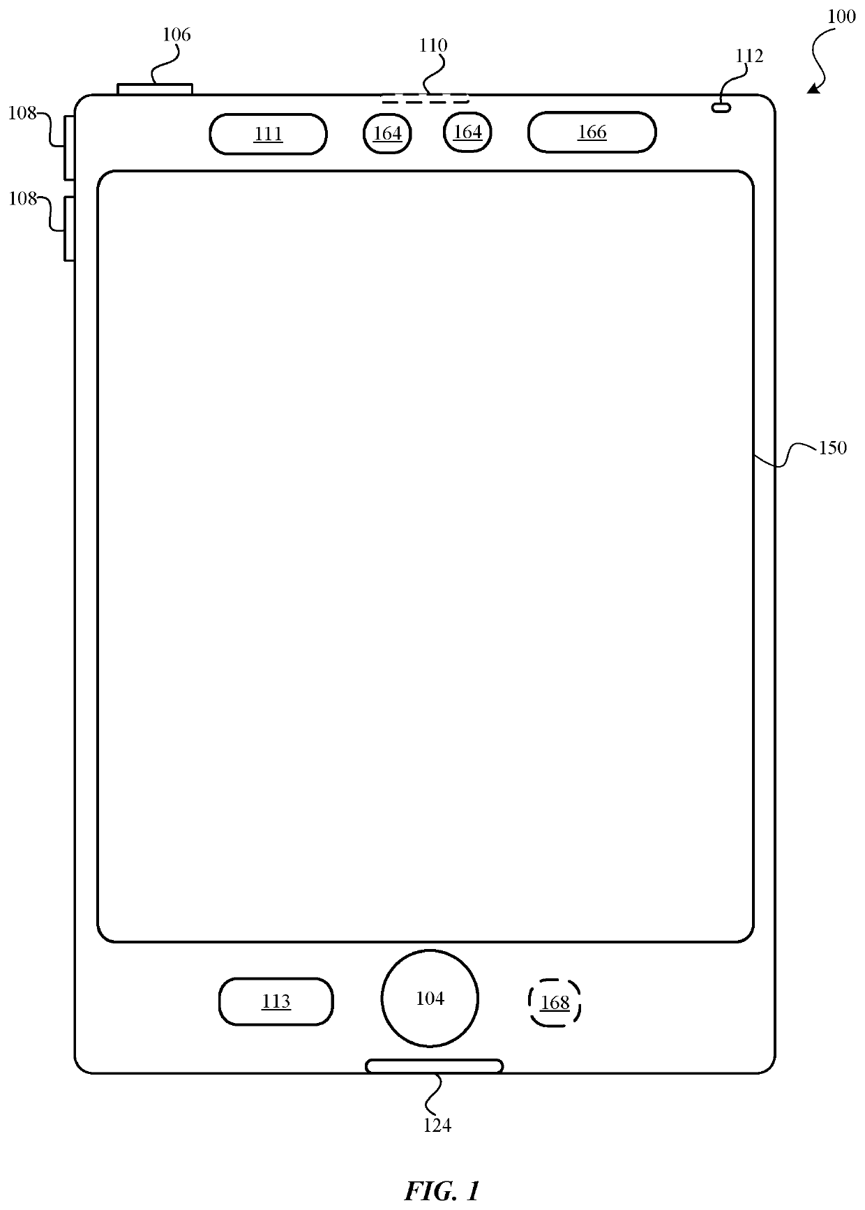
[0017]Embodiments of electronic devices, user interfaces for such devices, and associated processes for using such devices are described. In some embodiments, the device is a portable communications device, such as a mobile telephone, that also contains other functions, such as personal digital assistant (PDA) and / or music player functions. Exemplary embodiments of portable multifunction devices include, without limitation, the iPhone®, iPod Touch®, Apple Watch®, and iPad® devices from Apple Inc. of Cupertino, Calif. Other portable electronic devices, such as wearables, laptops or tablet computers, are optionally used. In some embodiments, the device is not a portable communications device, but is a desktop computer or other computing device that is not designed for portable use. In some embodiments, the disclosed electronic device may include a touch sensitive surface (e.g., a touch screen display and / or a touch pad). An example electronic device described below in conjunctio...

example communication

System in Electronic Device

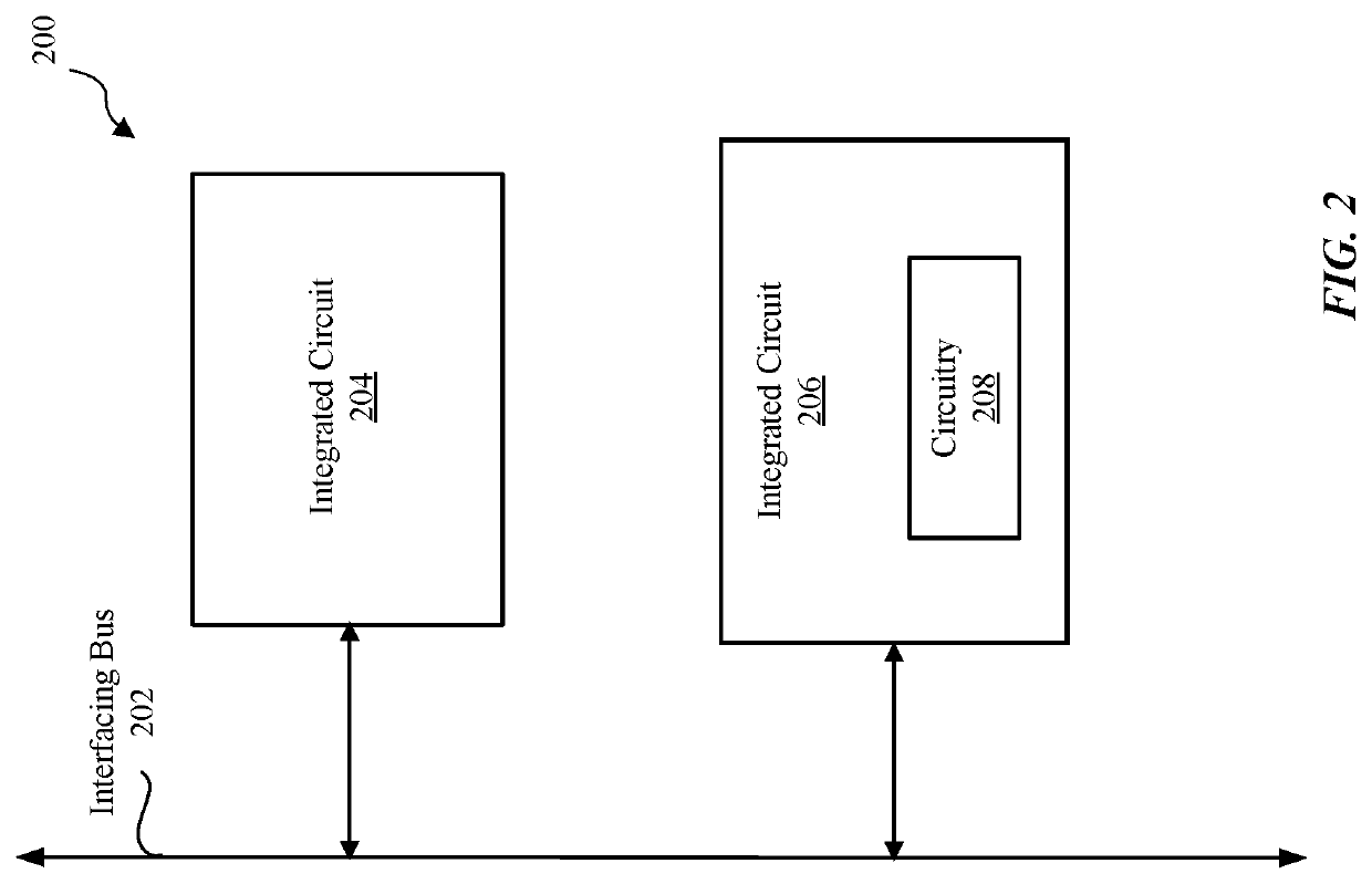
[0021]FIG. 2 is a block diagram illustrating components of electronic device 100 communicating over an interfacing bus 202, according to one embodiment. Electronic device 100 may include, among other components, an integrated circuit 204 and an integrated circuit 206 that communicate with each other via interfacing bus 202. The components illustrated in FIG. 2 may be part of, e.g., a communication subsystem in electronic device 100. Electronic device 100 may include additional components (e.g., user interfaces) not illustrated in FIG. 2.

[0022]Interfacing bus 202 is a communication channel that enables multiple components to communicate over a shared connection. In one or more embodiments, interfacing bus 202 is implemented as a multi-drop bus, which may be divided into more buses. For example, System Power Management Interface (SPMI) may be used to embody interfacing bus 202. Other serial bus interfaces such as I2C may be used instead of the SPMI to embody...


PUM


Abstract

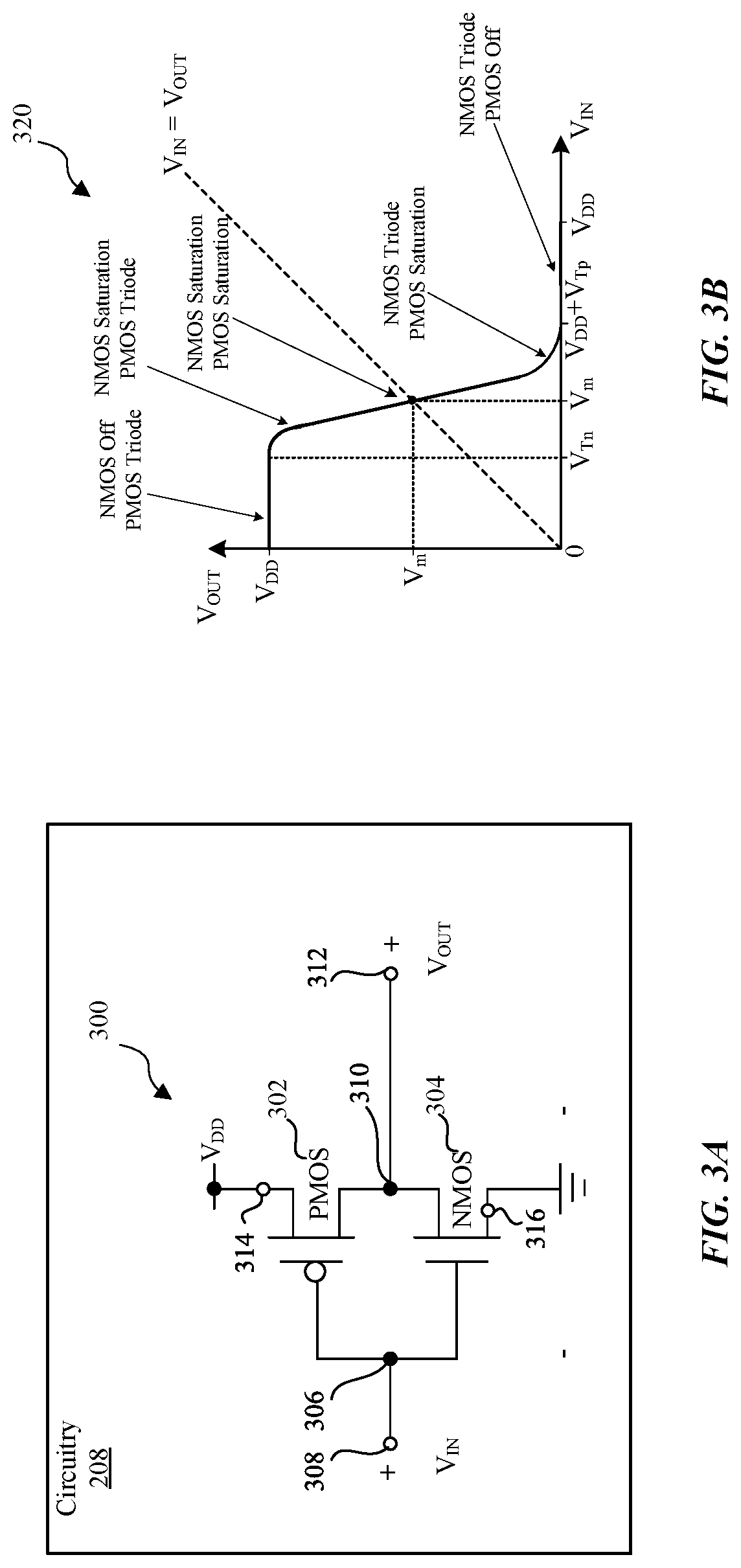
Embodiments relate to a circuitry for digital data communication. The circuitry includes an inverter circuit connected between an input node and an output node. The inverter circuit has core circuits each of which includes a complementary metal-oxide-semiconductor (CMOS) transistor of a first type and a CMOS transistor of a second type having a first common gate node connected to the input node and a first common drain node connected to the output node. The circuitry further includes another inverter circuit of a switching threshold voltage different than that of the inverter circuit and connected between the input node and the output node. The other inverter circuit has core circuits each of which includes a CMOS transistor of a third type and a CMOS transistor of a fourth type having a second common gate node connected to the input node and a second common drain node connected to the output node.

Description

BACKGROUND1. Field of the Disclosure[0001]The present disclosure relates to a complementary metal-oxide-semiconductor (CMOS) based receiver circuit that operates in a consistent manner despite supply voltage and temperature fluctuations.2. Description of the Related Art[0002]Integrated circuits for digital data communication typically include inverter based receiver circuits that include CMOS logic. A digital receiver that includes a CMOS based inverter circuit is easy to port across components and nodes implemented using different technologies, as well as across components operating under different conditions. The additional advantage of the receiver including the conventional CMOS based inverter circuit is that there is no static power consumption when the CMOS based inverter circuit is not utilized (e.g., disabled). However, operation of the conventional CMOS based inverter circuit is typically dependent on temperature as well as voltage supply ripples and other variations.SUMMAR...

Claims


Application Information

Patent Timeline
IPC IPC(8): H03K19/0948H03K19/00H04L13/18
CPCH03K19/0948H03K19/0027H04L13/18
Inventor EID, FAHMY MOHAMMEDCASTERS, JEROME
Owner APPLE INC
Learn More