Attaching an SMD to an insulating layer with a solder joint in a cavity formed in an insulating layer
a technology of insulating layer and solder joint, which is applied in the field of surface mount components, can solve the problems of premature removal of printed circuit boards, limited standoff, and damage of smd, and achieve the effects of increasing the associated standoff, simple operation, and increasing the service life of components
- Summary
- Abstract
- Description
- Claims
- Application Information
AI Technical Summary
Benefits of technology
Problems solved by technology
Method used
Image
Examples
first embodiment
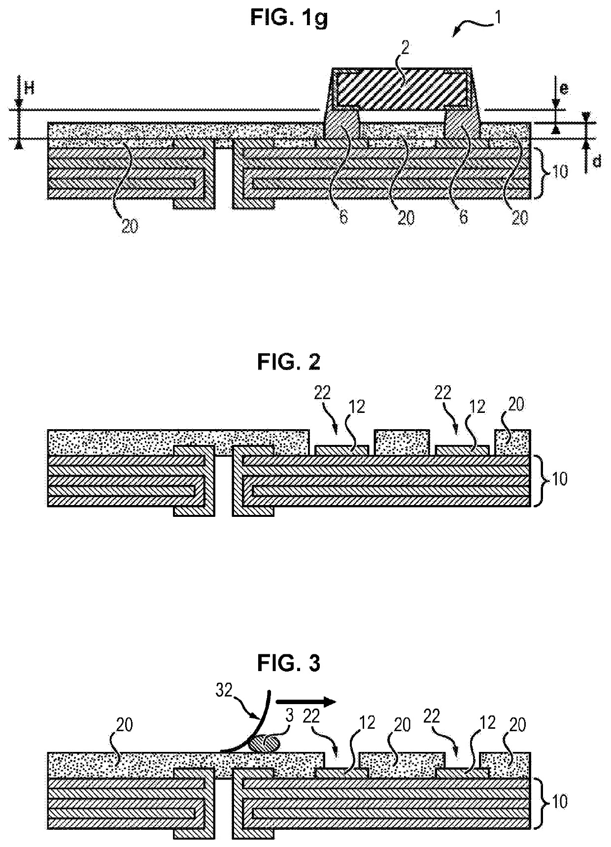
[0070]In a first embodiment, the insulating layer 20 can be applied by surface photolithography. In this case, the cavities 22 can also be formed by surface photolithography (see FIG. 2).
[0071]For this purpose, in a first step, a photoresist for forming the insulating layer 20 is applied to the connecting surface 14 in the form of a film. The resin can be a negative resin (ultraviolet radiation causes polymerization of the exposed areas, giving these areas a particular resistance to the developing solvent, while the noninsolated parts selectively disappear in this solvent) or a positive resin (ultraviolet radiation causes the macromolecules to break down, resulting in increased solubility of the exposed areas in the developing solvent). The resin may include an epoxy resin.
[0072]In a second step, a mask is applied to the resin film. The mask includes transparent and opaque areas to form the cavities 22 and the insulating layer 20.
[0073]In a third step, the resin film is exposed to l...
second embodiment
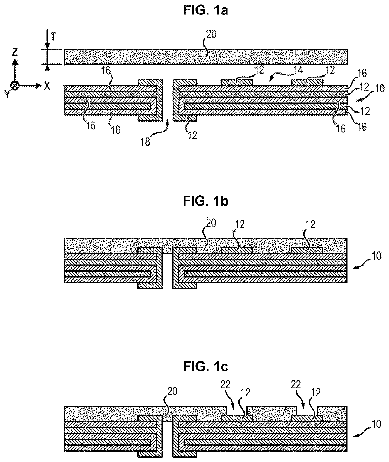
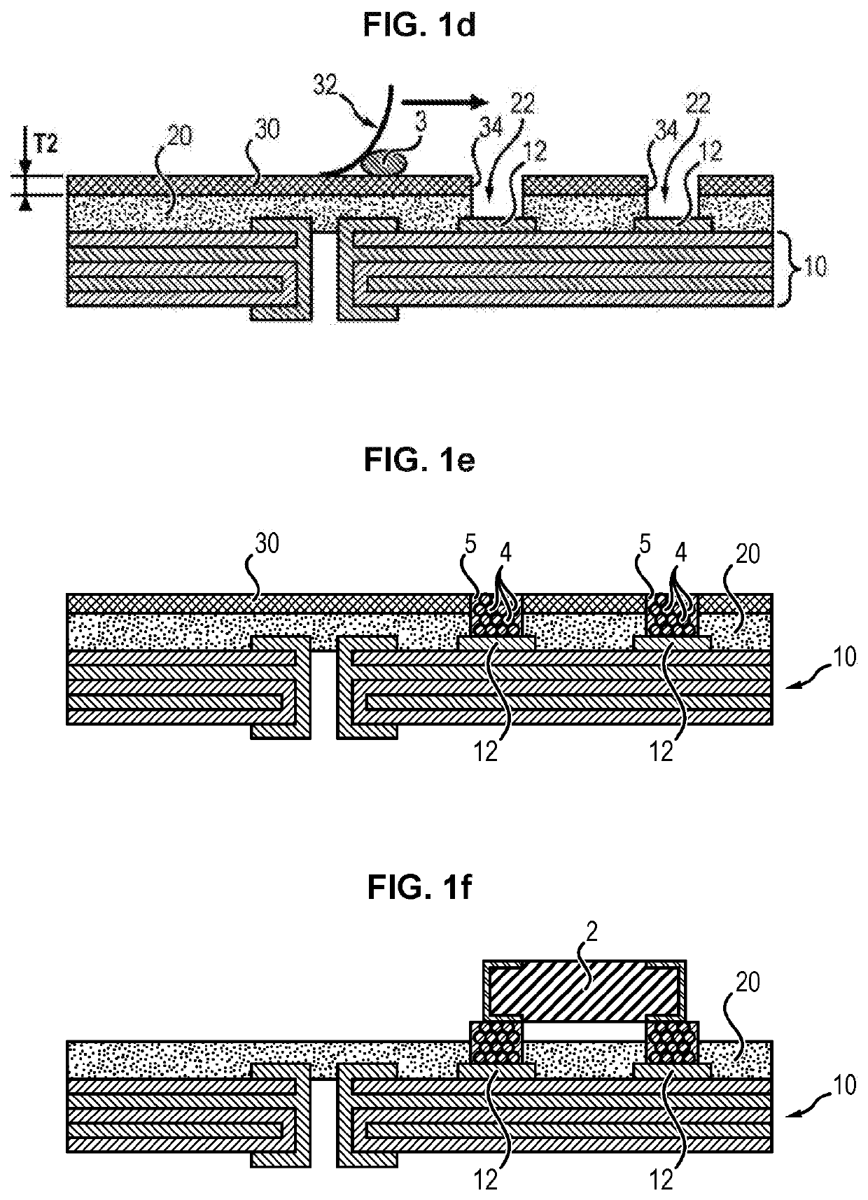
[0076]In a second embodiment, the insulating layer 20 can be applied and attached to the connecting surface 14, for example by lamination or gluing with an adhesive layer (see FIGS. 1a and 1b). The adhesive layer can include any type of adhesive material conventionally used in the printed circuit board industry to bond layers together, typically an epoxy adhesive.
[0077]The cavities 22 can then be preformed in the insulating layer 20 before it is placed on the connecting surface 14, or after it has been attached (as in FIG. 1c for example).
[0078]For example, the cavities 22 can be formed by cutting out insulating layer 20. Cutting can be done mechanically (using a cutting tool such as mechanical milling or mechanical drilling or laser drilling before placing on the surface 14). In the case of application on the surface 14 before the cavities are made, the cutting can be done by chemistry on dry or liquid photoimageable films or by mechanical milling or laser drilling. Laser drilling ...
PUM
| Property | Measurement | Unit |
|---|---|---|
| thickness | aaaaa | aaaaa |
| thickness | aaaaa | aaaaa |
| thickness | aaaaa | aaaaa |
Abstract
Description
Claims
Application Information


