One-transistor DRAM cell device having quantum well structure

a cell device and quantum well technology, applied in the field of one-transistor dynamic random access memory (1 t dram) cell devices, can solve the problems of capacitor scaling, large capacitor area occupied by the capacitor, capacitor scaling limitation, etc., and achieve the effect of reducing the area occupied by the device, increasing retention time, and limiting the channel length

Active Publication Date: 2021-10-26
GACHON UNIV OF IND ACADEMIC COOPERATION FOUND
View PDF19 Cites 1 Cited by
  • Summary
  • Abstract
  • Description
  • Claims
  • Application Information

AI Technical Summary

Benefits of technology

[0007]The present invention provides a 1T DRAM cell device having a quantum-well structure to solve the problems of the conventional 1T DRAM device. Particularly, it is to be manufactured by using the conventional CMOS technology on bulk silicon substrate. By forming a quantum well in the drain side of the channel with a heterojunction vertically and by using it as a charge storage layer, there is less restriction in the channel length, and the area occupied by the device can be more reduced than present. The write operation can be performed by gate-induced drain leakage (GIDL) or band-to-band tunneling, which enables low-power and high-speed operation capabilities, and dramatically improves retention time and read current margin.
[0026]In the present invention, by having two or more heterojunction surfaces perpendicular to the channel length direction and a quantum well at the drain side, the present invention can be driven by GIDL, band-to-band tunneling, and the like. It is possible to not only increase retention time, but also read current margin, and to operate as a memory device even in the harsh environment of high temperature.
[0027]In addition, since it is possible to form a heterojunction surface by vertically stacking epitaxial layers on a semiconductor substrate such as silicon, the conventional CMOS process technology can be used, and the area occupied by the device can be reduced as much as possible without limiting the channel length.

Problems solved by technology

The area occupied by the capacitor is very large compared to that of the transistor, and there is a big limitation in scaling the capacitor due to the charge sharing effect.
However, there are several difficulties in capacitor scaling because the number of materials that can be integrated with silicon (Si) is limited, research time and data accumulation for new materials are needed, and high-level process technology is required.
These difficulties hinder the scaling of DRAM.
However, the 1T DRAM devices proposed so far have similar or more deteriorated characteristics than the conventional 1T1C cells in terms of retention time and read current margin, which are important indicators of DRAM cell characteristics.
In addition, since most devices are based on SOI substrates and have difficulty in reducing cell size, there are many limitations in replacing the conventional DRAM.

Method used


Image

  • One-transistor DRAM cell device having quantum well structure
  • One-transistor DRAM cell device having quantum well structure
  • One-transistor DRAM cell device having quantum well structure

Examples


first embodiment

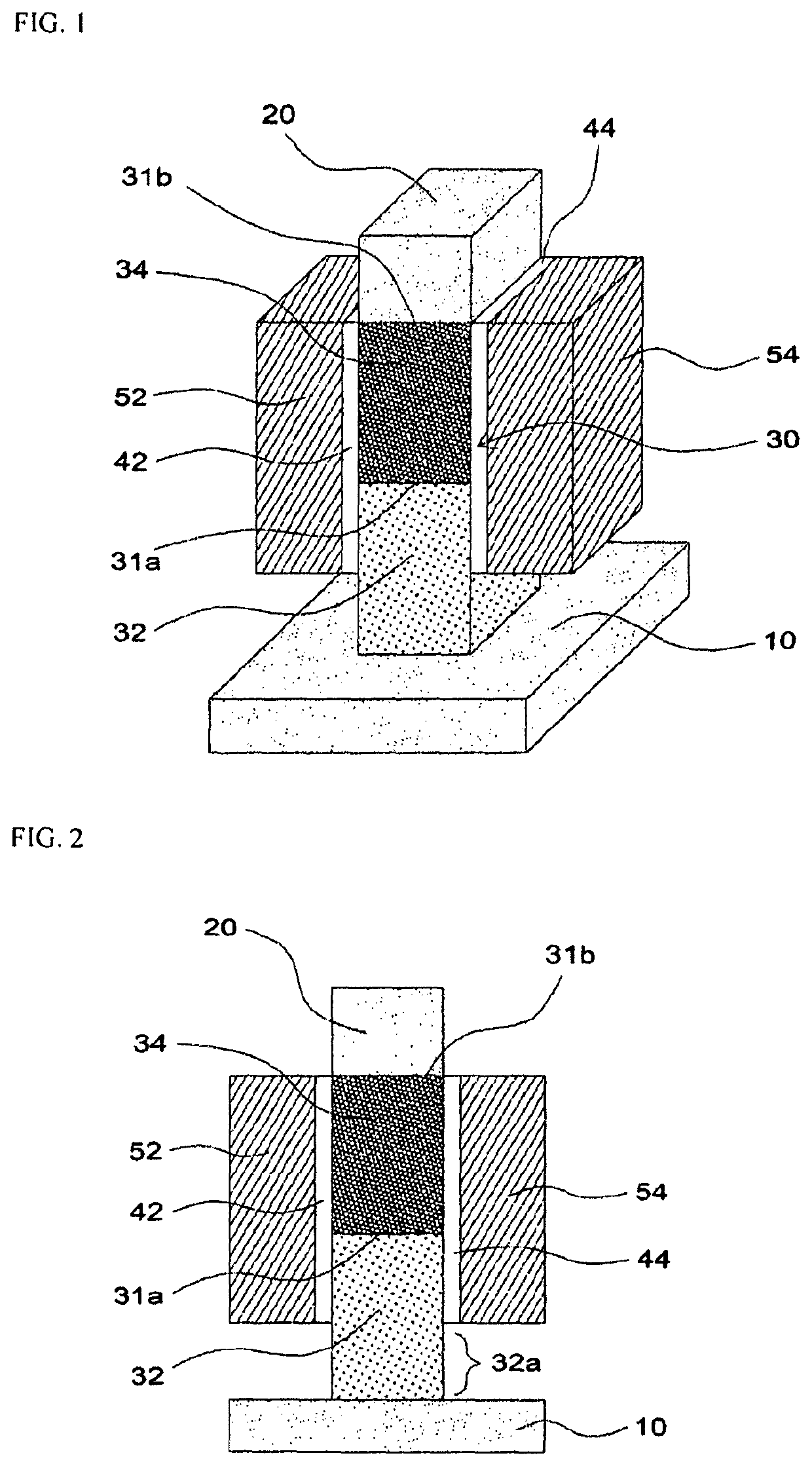
[0039]The 1T DRAM cell device according to the first embodiment of the present invention comprises, as shown in FIGS. 1 and 2, a body region 30 connecting a source region 10 and a drain region 20 and storing charge, and one or more gates 52 and 54 formed on the body region 30 with a gate insulating layer 42 or 44 interposed therebetween. Here, the body region 30 has a first semiconductor layer 32 and a second semiconductor layer 34 formed in a channel length direction with a first heterojunction surface 31a, and the first heterojunction surface 31a is perpendicular to the channel length direction.

[0040]The first semiconductor layer 32 may be formed of the same semiconductor material as that of the source region. It may have a homojunction with the source region 10. The second semiconductor layer 34 may be formed of a semiconductor material different from the drain region 20 to be in contact with a second heterojunction surface 31b perpendicular to the channel length direction.

[0041]...

second embodiment

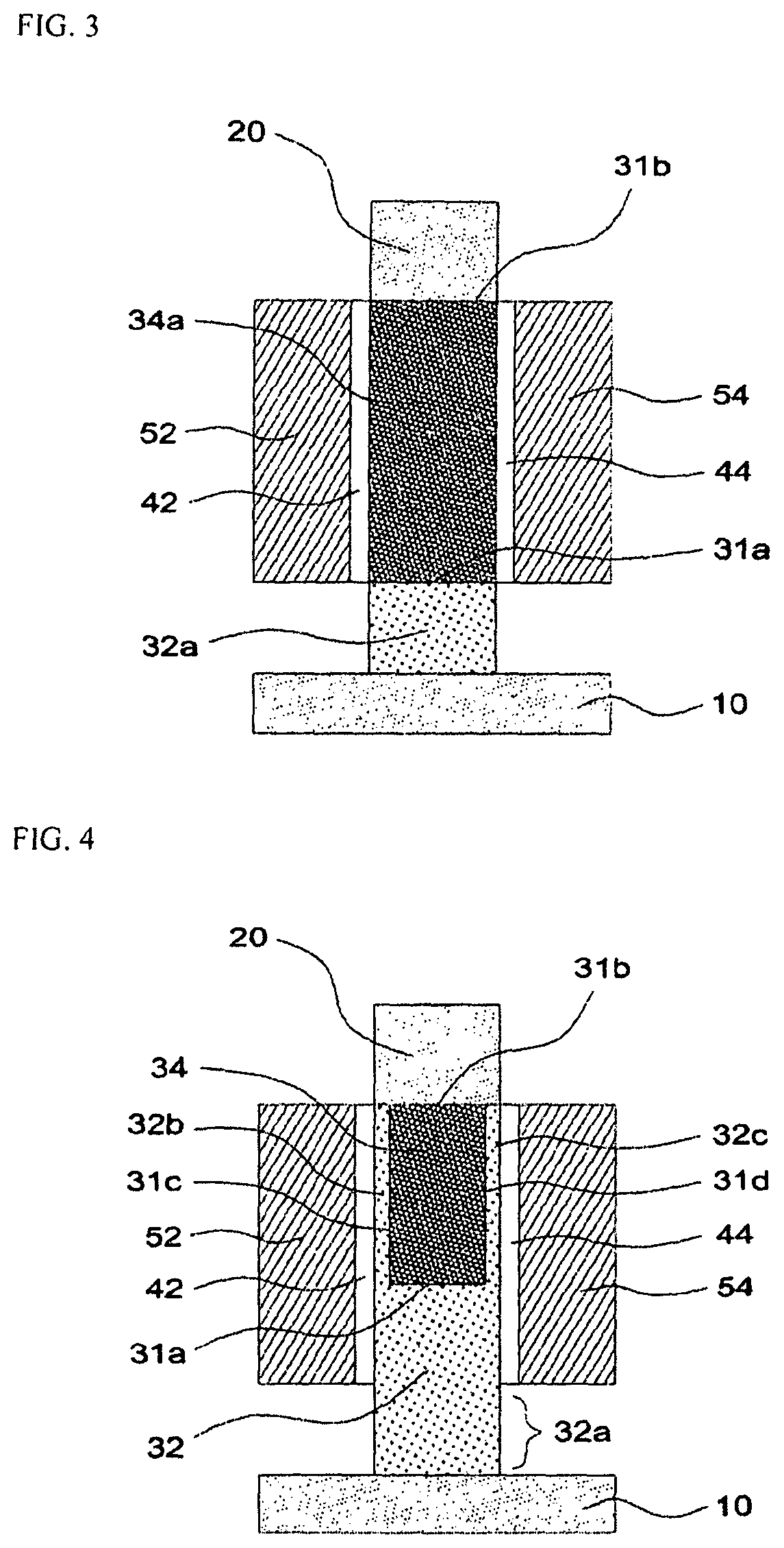
[0067]The 1T DRAM cell device according to the second embodiment of the present invention comprises, as shown in FIG. 3, a body region 30 connecting a source region 10 and a drain region 20 and storing charge, and one or more gates 52 and 54 formed on the body region 30 with a gate insulating layer 42 or 44 interposed therebetween. Here, the body region 30 has a first semiconductor layer 32 and a second semiconductor layer 34 formed in a channel length direction with a first heterojunction surface 31a, and the first heterojunction surface 31a is perpendicular to the channel length direction. Two or more gates 52 and 54 are formed on the second semiconductor layer 34a at a position spaced apart from the source region 10 by the first semiconductor layer 32a.

[0068]The rest of the configuration and application examples are the same as those of the first embodiment described above.

third embodiment

[0069]The 1T DRAM cell device according to the third embodiment of the present invention comprises, as shown in FIG. 4, a body region 30 connecting a source region 10 and a drain region 20 and storing charge, and one or more gates 52 and 54 formed on the body region 30 with a gate insulating layer 42 or 44 interposed therebetween. The body region 30 has a first semiconductor layer 32 and a second semiconductor layer 34 formed in a channel length direction, the second semiconductor layer 34 being inserted in the first semiconductor layer 32 with a predetermined length from one side of the drain 20 in the channel length direction and having a first heterojunction surface 31a perpendicular to the channel length direction and one or more third heterojunction surfaces 31c and 31d parallel to the channel length direction. The second semiconductor layer 34 is formed of a semiconductor material different from the drain region 20 to be in contact with a second heterojunction surface 31b perp...


PUM

PropertyMeasurementUnit
energy bandaaaaaaaaaa
timeaaaaaaaaaa
dielectric constantaaaaaaaaaa

Abstract

A 1T DRAM cell device having two or more heterojunction surfaces perpendicular to the channel length direction and a quantum well at the drain region side. The 1T DRAM cell device described herein may be driven by GIDL or band-to-band tunneling, so that low voltage and high speed operation can be performed, and retention time and read current margin can be dramatically increased. It can also be driven as a memory device in harsh environments with high temperatures. Furthermore, since the heterojunction surfaces can be formed by vertically stacking epitaxial layers on a semiconductor substrate such as silicon, the conventional CMOS process technology can be used, and the area occupied by the device can be reduced as much as possible without limiting the channel length.

Description

CROSS-REFERENCE TO RELATED APPLICATION[0001]This application claims priority to Korean Patent Application No. 10-2018-0127746, filed on Oct. 24, 2018, under 35 U.S.C. 119, the entire contents of which are hereby incorporated by reference.BACKGROUND[0002]Field of the Invention. The present invention relates to a semiconductor memory device, and more particularly to a one-transistor dynamic random access memory (1T DRAM) cell device having a quantum-well structure by heterojunction without a capacitor.[0003]Related Art. Currently, a unit cell of DRAM is composed of one transistor and one capacitor (1T1C). The area occupied by the capacitor is very large compared to that of the transistor, and there is a big limitation in scaling the capacitor due to the charge sharing effect.[0004]Therefore, DRAM scaling is being made in the direction of developing a high dielectric constant insulator for a capacitor and increasing the aspect ratio of the capacitor. However, there are several difficul...

Claims


Application Information

Patent Timeline
Patent Type & Authority Patents(United States)
IPC IPC(8): H01L29/78H01L29/66H01L27/108H01L29/12H01L29/165
CPCH01L29/66977H01L27/108H01L29/122H01L29/165H01L29/7827H01L29/7831H01L29/1054H01L29/1045H01L29/1041H01L29/7391H10B12/00H01L21/823807H01L29/41725H10B12/30
Inventor CHO, SEONGJAEYU, EUNSEONLEE, JAE YOON
Owner GACHON UNIV OF IND ACADEMIC COOPERATION FOUND
Why Eureka
Try Eureka