Chip package structure and manufacturing method thereof

a technology of chip packaging and manufacturing method, applied in the direction of semiconductor devices, semiconductor/solid-state device details, electrical apparatus, etc., can solve the problems of increased manufacturing costs, reduced circuit board size, and difficulty in handling and moving, so as to reduce manufacturing costs, increase product yield, and facilitate manufacturing.

Active Publication Date: 2021-11-30
HO CHUNG W
View PDF5 Cites 0 Cited by
  • Summary
  • Abstract
  • Description
  • Claims
  • Application Information

AI Technical Summary

Benefits of technology

[0005]The invention provides a chip package structure and a manufacturing method thereof, which are safer and easier in terms of manufacturing, can effectively reduce manufacturing costs and increase product yields, and have better heat dissipation and anti-electromagnetic interference effects.

Problems solved by technology

However, in the well-known coreless manufacturing process, since some of the carrier board and some of the circuit board require to be cut off, the size of the circuit board may be reduced and the cut-off carrier board cannot be reused, resulting in increased manufacturing costs.
However, since the stainless steel board is of a heavy weight, during the manufacturing process, handling and moving may often be difficult.
Moreover, edges and corners thereof are relatively sharp, often causing damage to the manufacturing equipment.
In addition, for most package structures, electromagnetic interference (EMI) is a common but unfavorable interference, and the interference may be interruption, hindrance, reduction, or limitation of the overall performance of the circuit.
In the conventional art, generally, after completion of the packaging, a metal coating on the outside of the molding compound is manufactured by electroplating or sputtering to serve to improve the electromagnetic interference shielding performance of the package structure, but this results in a thickened package structure and higher process costs.

Method used


Image

  • Chip package structure and manufacturing method thereof
  • Chip package structure and manufacturing method thereof
  • Chip package structure and manufacturing method thereof

Examples


Embodiment Construction

[0034]Reference will now be made in detail to the exemplary embodiments of the invention, examples of which are illustrated in the accompanying drawings. Wherever possible, the same reference numerals are used in the drawings and description to represent the same or similar parts.

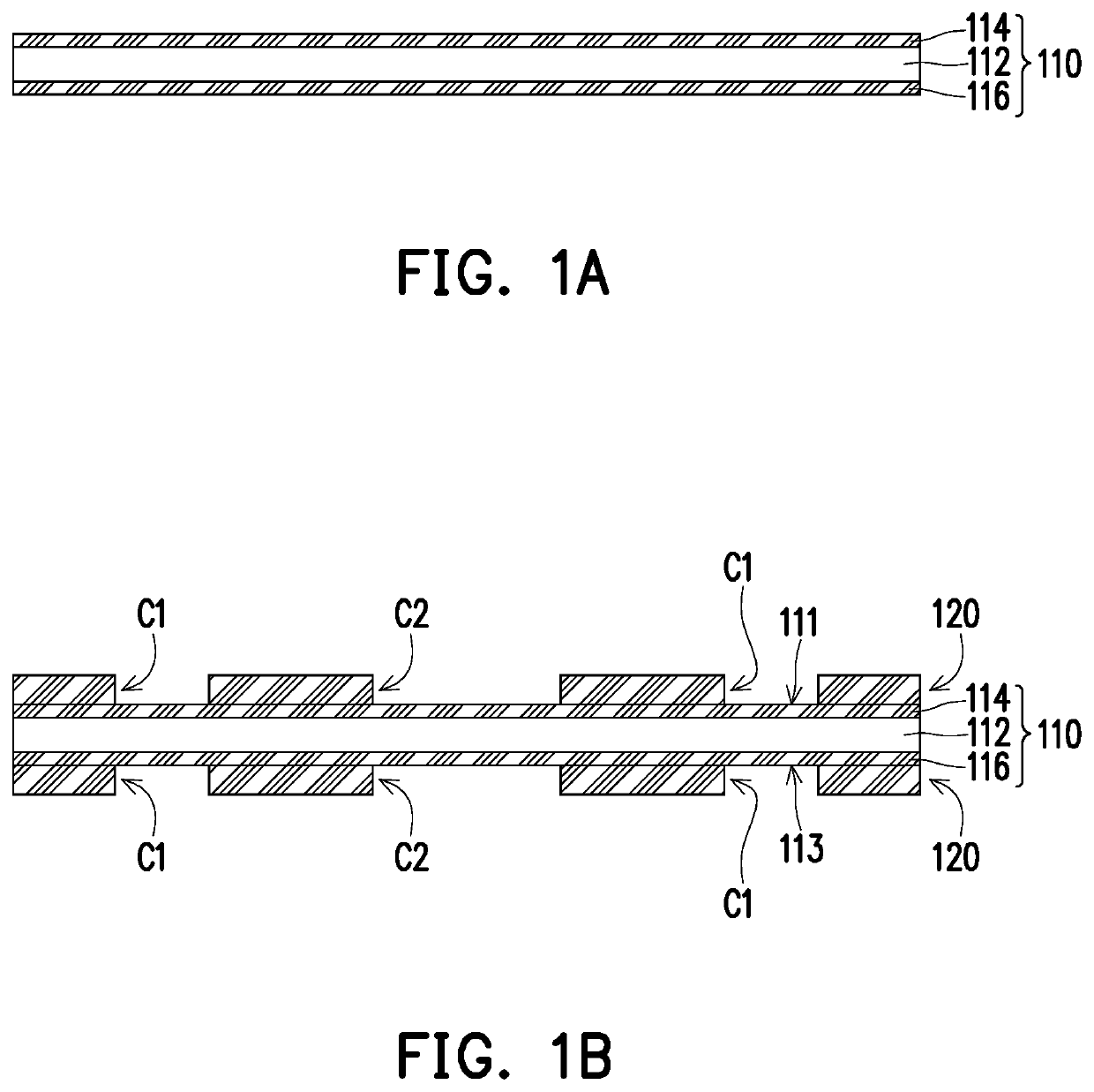
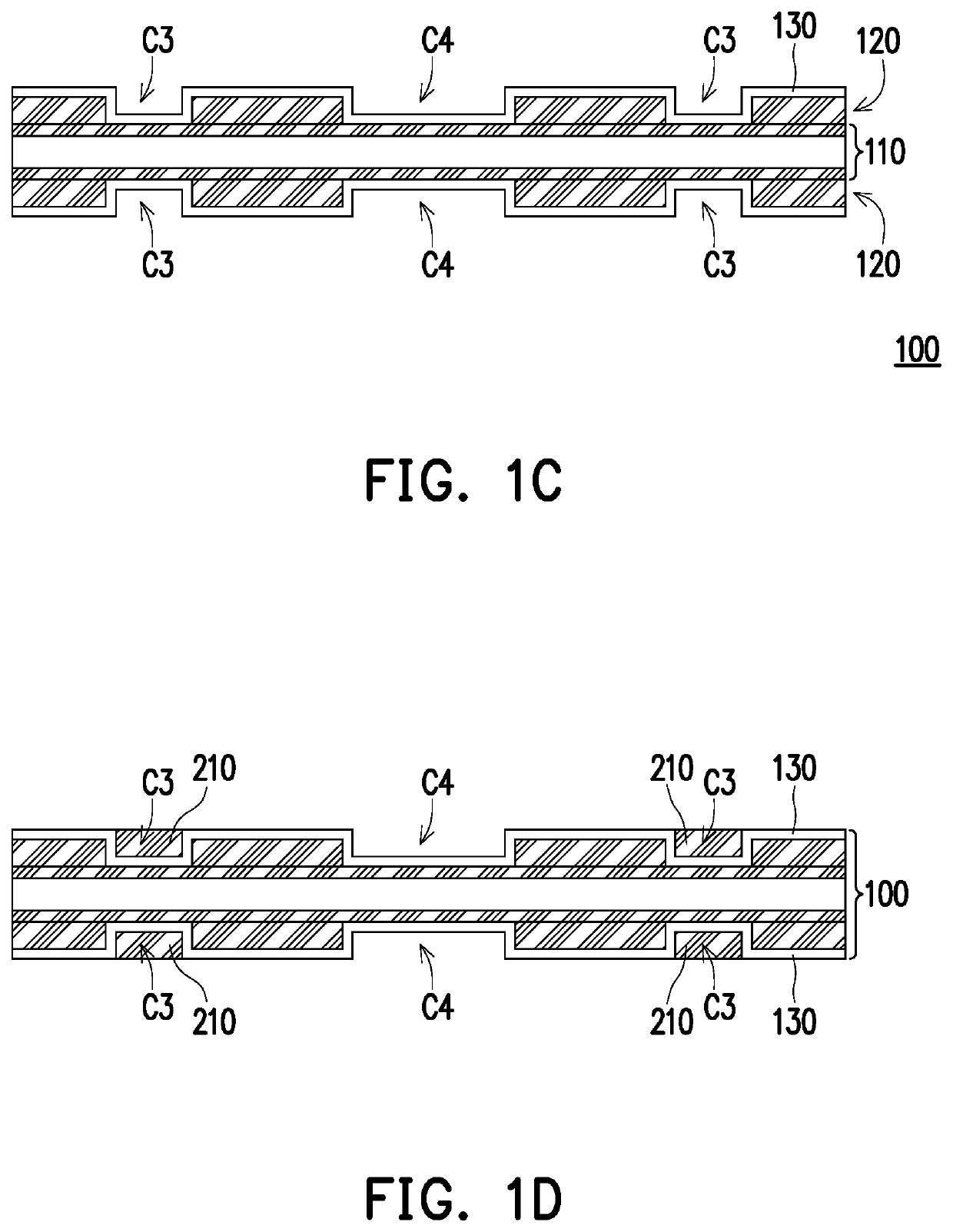
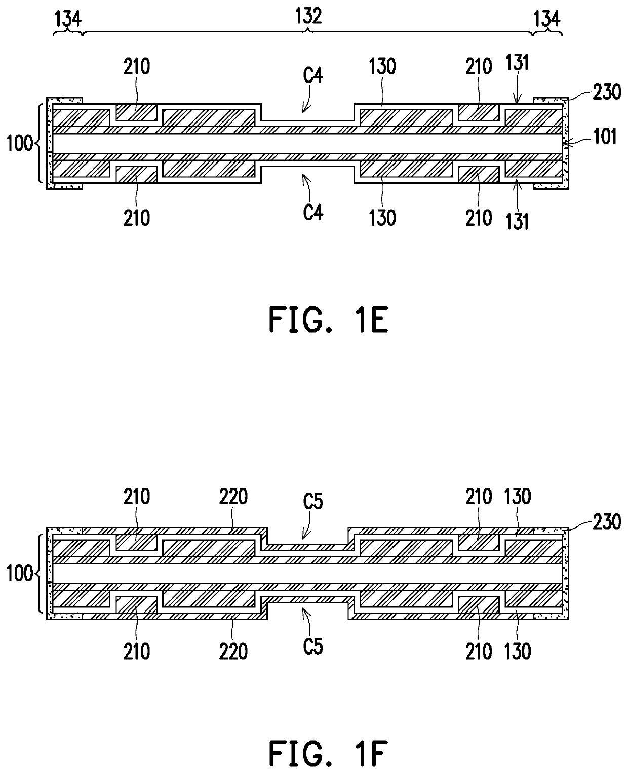
[0035]FIG. 1A to FIG. 1J are schematic cross-sectional views of a manufacturing method of a chip package structure of an embodiment of the invention. Regarding the manufacturing method of the chip package structure of this embodiment, first, with reference to FIG. 1F, a carrier board 100 having a plurality of conductive blocks 210 and at least one metal layer 220 formed thereon (two metal layers 220 being schematically shown) is provided. Specifically, with reference to FIG. 1A, a substrate 110 is provided, and the substrate 110 includes a core layer 112, a first conductive layer 114, and a second conductive layer 116. The first conductive layer 114 and the second conductive layer 116 are respectively dispo...


PUM

PropertyMeasurementUnit
thicknessaaaaaaaaaa
thicknessaaaaaaaaaa
depthaaaaaaaaaa

Abstract

A manufacturing method a chip package structure. The carrier board includes a substrate and a stainless steel layer sputtered on the substrate. The substrate has multiple first cavities and at least one second cavity. The stainless steel layer conformally covers the first cavities and the second cavity to define multiple third cavities and at least one fourth cavity. Conductive blocks fill the third cavities. At least one metal layer covers the stainless steel layer, the conductive blocks, and the fourth cavity to define at least one fifth cavity. At least one chip is disposed inside the fifth cavity. At least one circuit structure layer is formed on the carrier board. A patterned circuit layer of the circuit structure layer is electrically connected with multiple electrodes of the chip. The carrier board and the circuit structure layer are separated to expose the conductive blocks and the metal layer.

Description

TECHNICAL FIELD[0001]The invention relates to a package structure and a manufacturing method thereof, and particularly, to a chip package structure and a manufacturing method thereof.DESCRIPTION OF RELATED ART[0002]In the well-known coreless manufacturing process, part of the edge of the carrier board and part of the edge of the circuit board are first bonded with adhesive or copper-plated edge sealing. In another convention, a thin substrate (with a thickness of 100 μm, for example) containing a glass fiber cloth and, on each of both sides, being adhered with a piece of copper foil and a peelable ultra-thin copper foil (with a thickness of 3 μm to 5 μm, for example) attached thereon is employed as a carrier board. After the circuit board undergoes several processes, the part with adhesive or copper-plated edge sealing between the carrier board and the circuit board is cut off to obtain the circuit board for packaging process. However, in the well-known coreless manufacturing proces...

Claims


Application Information

Patent Timeline
Patent Type & Authority Patents(United States)
IPC IPC(8): H01L21/56H01L23/552H01L23/31H01L23/00
CPCH01L21/568H01L21/561H01L23/3135H01L23/552H01L24/05H01L2224/05624H01L2224/05647H01L2224/04105H01L2924/3025H01L21/4857H01L23/49822H01L2224/95H01L24/19H01L24/95H01L24/20H01L2224/19H01L2224/2105H01L2224/214
Inventor HO, CHUNG W.
Owner HO CHUNG W
Why Eureka
Try Eureka