Dielectric fins with different dielectric constants and sizes in different regions of a semiconductor device

a technology of dielectric fins and semiconductor devices, applied in the field of semiconductor integrated circuits, can solve the problems of increasing the complexity of processing and manufacturing ics, not optimizing the performance of conventional ics, and not being entirely satisfactory in every asp

Active Publication Date: 2022-03-22
TAIWAN SEMICON MFG CO LTD
View PDF20 Cites 0 Cited by
  • Summary
  • Abstract
  • Description
  • Claims
  • Application Information

AI Technical Summary

Benefits of technology

[0075]Based on the above discussions, it can be seen that the present disclosure offers advantages over conventional FinFET devices. It is understood, however, that other embodiments may offer additional advantages, and not all advantages are necessarily disclosed herein, and that no particular advantage is required for all embodiments. One advantage is that the shorter height the dielectric fins (which may be a hybrid structure) in the sparse region allows the source / drain epi-layers in the sparse region to not be otherwise constrained by the dielectric fins. Bridging is unlikely to occur anywhere in the sparse region, since the device fins (and therefore the epi-layers grown thereon) are sufficiently spaced apart from one another. The full growth of the source / drain epi-layers in the sparse region optimizes parameters such as epi-stress, larger surface area for silicide formation, increased contact landing window, etc., thereby enhancing the performance of the devices in the sparse region. Another advantage is that electrical bridging is still prevented in the dense region, since dielectric fins in the dense region are still tall enough to block the lateral merging of source / drain epi-layers. Furthermore, the different dielectric constants of the dielectric fins in the sparse and dense regions help to optimize performance as well. For example, the relatively low dielectric constant of the dielectric fin in the sparse region means that the parasitic capacitance will be lower, which results in a faster device speed, especially for high frequency applications. Meanwhile, the relatively high dielectric constant of the dielectric fin in the dense region means that these dielectric fins are more effective at providing electrical isolation for the adjacent source / drain epi-layers in the dense region. In this manner, the present disclosure simultaneously alleviates the different concerns and optimizes different criteria for devices in both the sparse region and the dense region. Other advantages include compatibility with existing FinFET fabrication, so the present disclosure does not require additional processing and is therefore easy and cheap to implement.

Problems solved by technology

However, such scaling down has also increased the complexity of processing and manufacturing ICs and, for these advances to be realized.
However, conventional ICs typically have a “one-size-fits-all” approach with respect to the implementation of dielectric fins, which does not optimize the performance of the conventional ICs.
Therefore, while existing FinFET devices and the fabrication thereof have been generally adequate for their intended purposes, they have not been entirely satisfactory in every aspect.

Method used


Image

  • Dielectric fins with different dielectric constants and sizes in different regions of a semiconductor device
  • Dielectric fins with different dielectric constants and sizes in different regions of a semiconductor device
  • Dielectric fins with different dielectric constants and sizes in different regions of a semiconductor device

Examples


Embodiment Construction

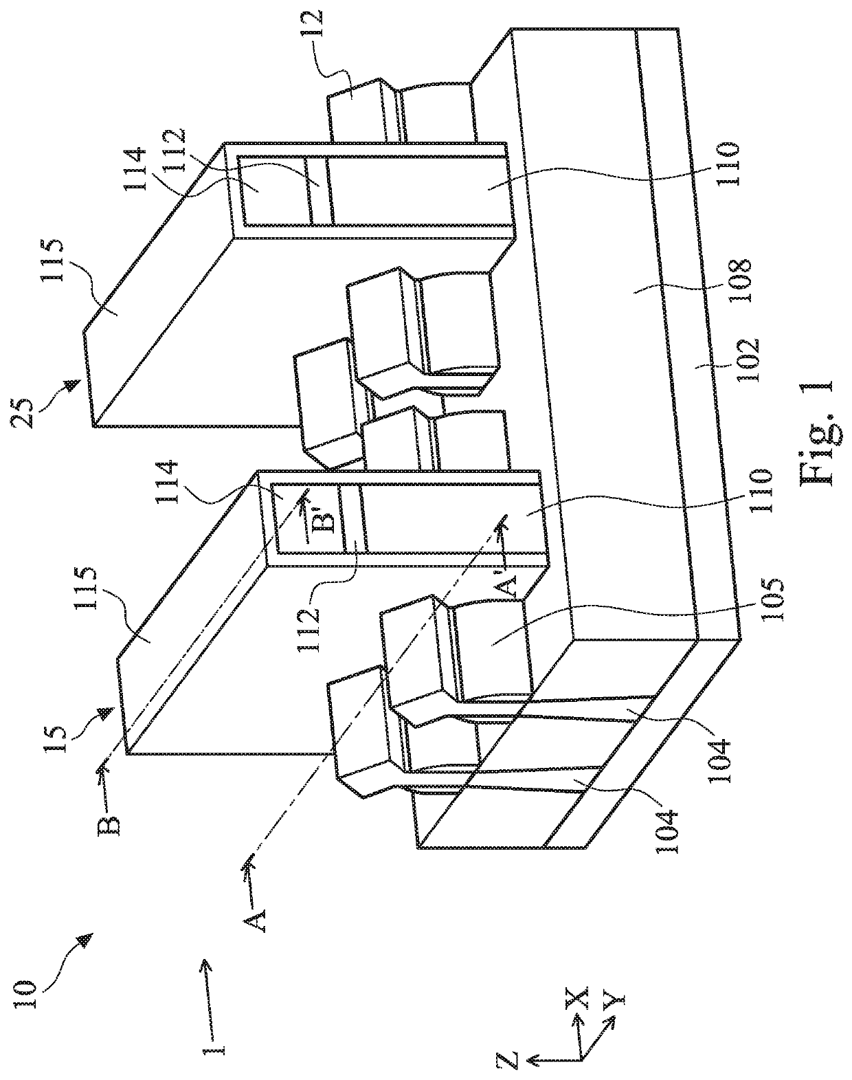
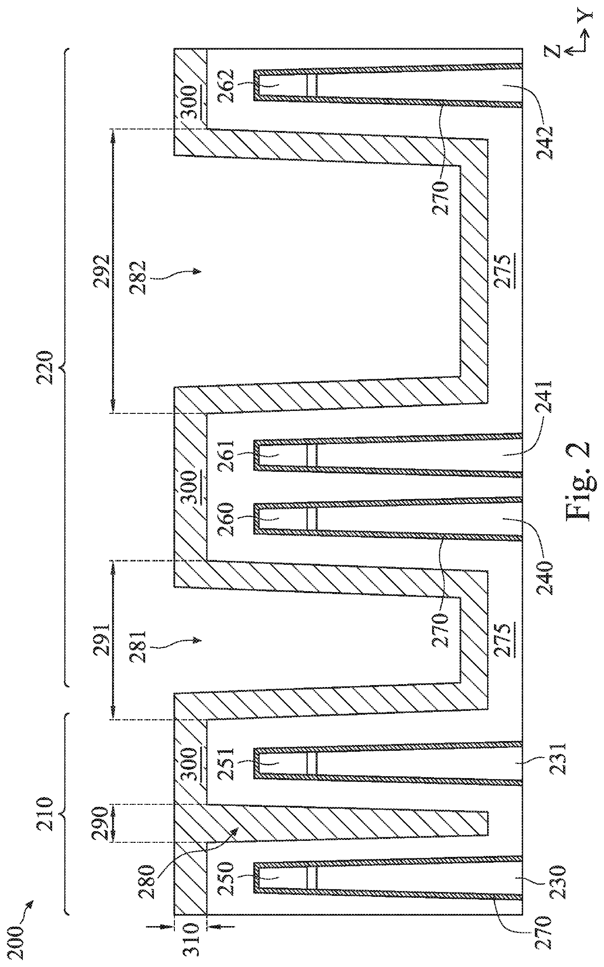
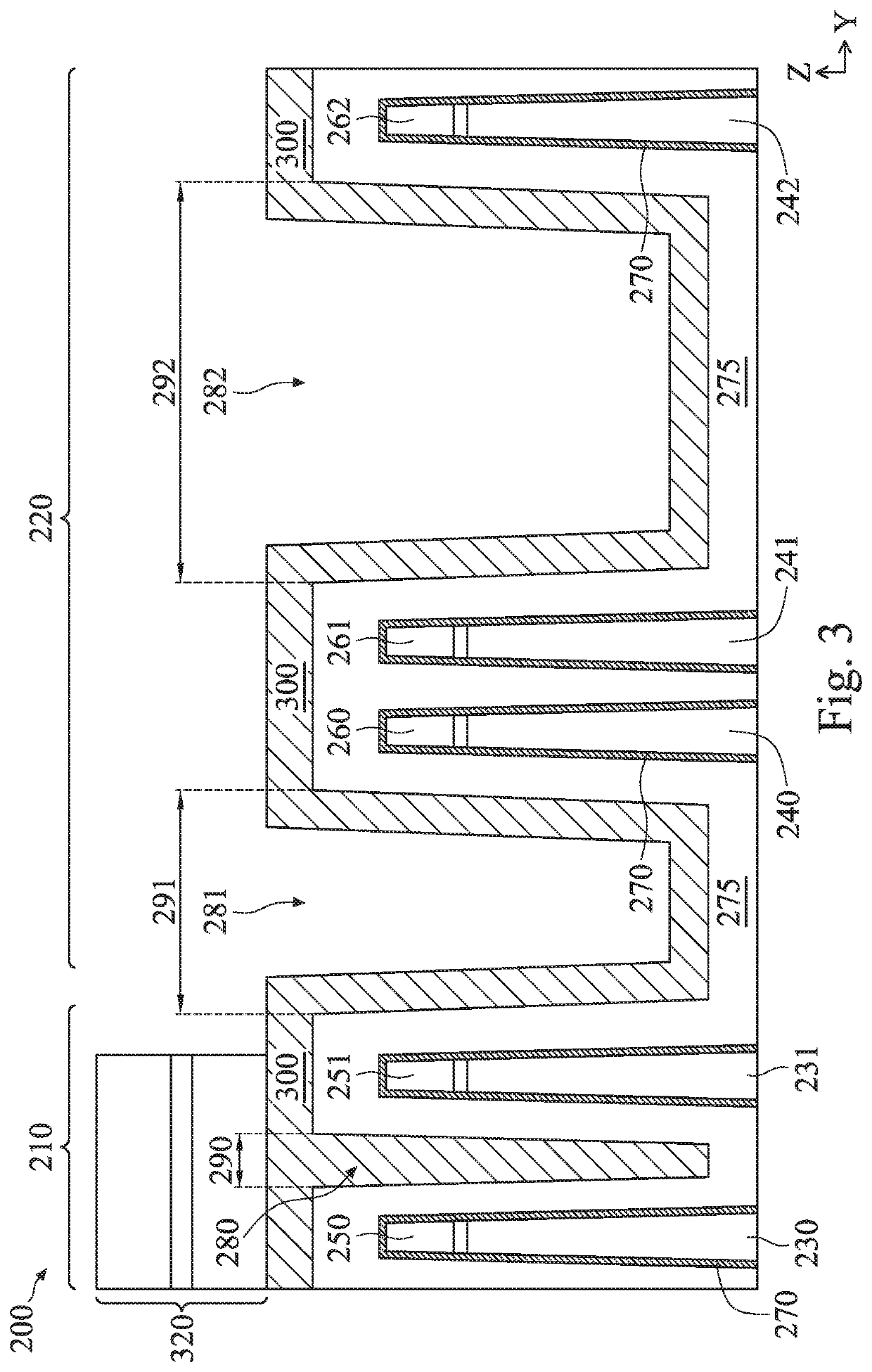
[0011]The following disclosure provides many different embodiments, or examples, for implementing different features of the provided subject matter. Specific examples of components and arrangements are described below to simplify the present disclosure. These are, of course, merely examples and are not intended to be limiting. For example, the formation of a first feature over or on a second feature in the description that follows may include embodiments in which the first and second features are formed in direct contact, and may also include embodiments in which additional features may be formed between the first and second features, such that the first and second features may not be in direct contact. In addition, the present disclosure may repeat reference numerals and / or letters in the various examples. This repetition is for the purpose of simplicity and clarity and does not in itself dictate a relationship between the various embodiments and / or configurations discussed.

[0012]F...


PUM

PropertyMeasurementUnit
dielectric constantaaaaaaaaaa

Abstract

A semiconductor device includes. A first epi-layer and a second epi-layer are each located in a first region of the semiconductor device. A first dielectric fin is located between the first epi-layer and the second epi-layer. The first dielectric fin has a first dielectric constant. A third epi-layer and a fourth epi-layer are each located in a second region of the semiconductor device. A second dielectric fin is located between the third epi-layer and the fourth epi-layer. The second dielectric fin has a second dielectric constant that is less than the first dielectric constant.

Description

PRIORITY DATA[0001]The present application is a U.S. Utility Patent Application of U.S. Provisional Patent Application No. 62 / 750,948, filed on Oct. 26, 2018, the disclosure of which is hereby incorporated by reference in its entirety.BACKGROUND[0002]The semiconductor integrated circuit (IC) industry has experienced exponential growth. Technological advances in IC materials and design have produced generations of ICs where each generation has smaller and more complex circuits than the previous generation. In the course of IC evolution, functional density (i.e., the number of interconnected devices per chip area) has generally increased while geometry size (i.e., the smallest component (or line) that can be created using a fabrication process) has decreased. This scaling down process generally provides benefits by increasing production efficiency and lowering associated costs.[0003]However, such scaling down has also increased the complexity of processing and manufacturing ICs and, f...

Claims


Application Information

Patent Timeline
Patent Type & Authority Patents(United States)
IPC IPC(8): H01L21/8234H01L21/762H01L21/3105H01L27/088
CPCH01L21/823481H01L21/31053H01L21/762H01L27/0886H01L29/7856H01L29/66795H01L29/0688H01L21/823418H01L21/823431H01L29/7855H01L29/4236H01L29/408H01L29/66348
Inventor HSIEH, MIN-YANNCHEN, HUA FENGLIAW, JHON JHY
Owner TAIWAN SEMICON MFG CO LTD
Why Eureka
Try Eureka