Chip-scale packaging light-emitting device with electrode polarity identifier and method of manufacturing the same

a technology of light-emitting devices and chip-scale packaging, which is applied in the direction of semiconductor devices, basic electric elements, electrical appliances, etc., can solve the problems of slowing down the manufacturing process, difficult to determine the orientation of the light-emitting semiconductor chips disposed inside the csp led either by human eyes or by machine vision, and inability to readily distinguish the anode and the cathode of the light-emitting semiconductor chips from the appearan

Active Publication Date: 2022-05-17
MAVEN OPTRONICS CO LTD
View PDF33 Cites 0 Cited by
  • Summary
  • Abstract
  • Description
  • Claims
  • Application Information

AI Technical Summary

Benefits of technology

[0008]An object of some embodiments of the present disclosure is to provide a CSP LED having an electrode polarity identifier which can be used to recognize the orientation of the electrode polarity, and a manufacturing method thereof, wherein the manufacturing yield to fabricate the CSP LED with an electrode polarity identifier is not adversely affected.
[0017]Thereby, the CSP LED and the manufacturing method thereof disclosed according to some embodiments of the present disclosure can provide at least the following technical benefits. (1). When viewed from the top side or the bottom side of a CSP LED, the CSP LED exhibits a first region and a second region of different area sizes and has an asymmetric appearance of the different area sizes, whereby the asymmetric regions can be readily recognized visually by human eyes or machine vision so that an orientation of the electrode polarity can be identified. (2). The feature of asymmetric appearance exhibited by the CSP LED with an electrode polarity identifier can be readily fabricated using a single singulation manufacturing process such as cutting or molding. Because the singulation process is an already-included manufacturing stage to fabricate a CSP LED without an electrode polarity identifier, no additional manufacturing stage is added. Therefore, the manufacturing yield and the manufacturing cost to fabricate a CSP LED with an electrode polarity identifier are not affected. (3). The asymmetric appearance feature exhibited by the CSP LED with an electrode polarity identifier can be achieved without additionally including or injecting an additional amount of filler materials, and thus does not affect the manufacturing yield of the CSP LED. (4). When the packaging structure of a CSP LED with an electrode polarity identifier comprises a photoluminescent layer and a reflective structure, and the reflective structure is specified to cover the light-emitting semiconductor chip and the photoluminescent layer along a first horizontal direction, the first region and the second region of different area sizes can be specified on the reflective structure. Therefore, the difference in the area between the first region and the second region can be achieved by specifying different thicknesses of the reflective structure, so that the shape of the photoluminescent layer is still specified to be symmetrical and the optical characteristics of the LED are not affected accordingly. In other words, the appearance of a CSP LED with an electrode polarity identifier can be asymmetrical; however, the shape of the photoluminescent layer still has a symmetrical appearance. Because the photoluminescant layer is specified for wavelength and color conversion and the reflective structure is specified to provide a reflective surface, the light radiation pattern is not affected by the appearance of the asymmetric reflective structure after the primary light radiated by the light-emitting semiconductor chip passes through the photoluminescent layer.

Problems solved by technology

However, since a CSP LED has a small form factor and does not use an additional submount such as a ceramic submount, a printed circuit board (PCB) submount or a lead frame, an anode and a cathode of a light-emitting semiconductor chip cannot be readily distinguished from the appearance and the orientation of a CSP LED, either viewed from the top side or viewed from the bottom side.
It is therefore difficult to determine the orientation of the anode and cathode of the light-emitting semiconductor chip disposed inside the CSP LED either by human eyes or by machine vision.
Even though the orientation of the anode and cathode can be identified when a CSP LED is viewed from the bottom side using a high-magnification lens for machine vision, it slows down the manufacturing throughput and involves tedious manufacturing processes during a welding procedure to assemble CSP LEDs on application boards, such as flipping, arranging, and soldering CSP LEDs to the PCB, resulting in a low manufacturing efficiency of the welding procedure.
Further, once a CSP LED is arranged and disposed on the circuit board, it is difficult to identify the orientation of the anode and cathode from its appearance, and it is difficult to recognize whether the orientations of the CSP LEDs electrodes are correctly placed on the circuit board.
However, since the surface area of the phosphor layer of a CSP LED itself is already small, it is difficult to form an even finer recessed line mark or concave groove mark on the layer.
It is even more difficult to refill other materials to the recessed line mark or the concave groove mark due to the extremely small size of the recessed line mark or the concave groove mark.
Furthermore, the uncured filler material is difficult to flow into the recessed line mark or the concave groove mark, so that the filler material does not adequately fill up the concave groove mark in a flush manner, or the filler material overflows outside the concave groove mark.

Method used


Image

  • Chip-scale packaging light-emitting device with electrode polarity identifier and method of manufacturing the same
  • Chip-scale packaging light-emitting device with electrode polarity identifier and method of manufacturing the same
  • Chip-scale packaging light-emitting device with electrode polarity identifier and method of manufacturing the same

Examples


Embodiment Construction

Definitions

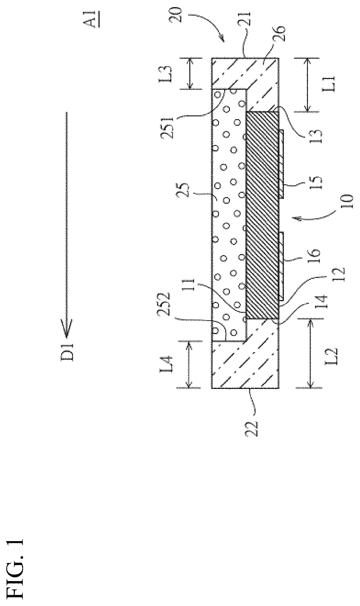
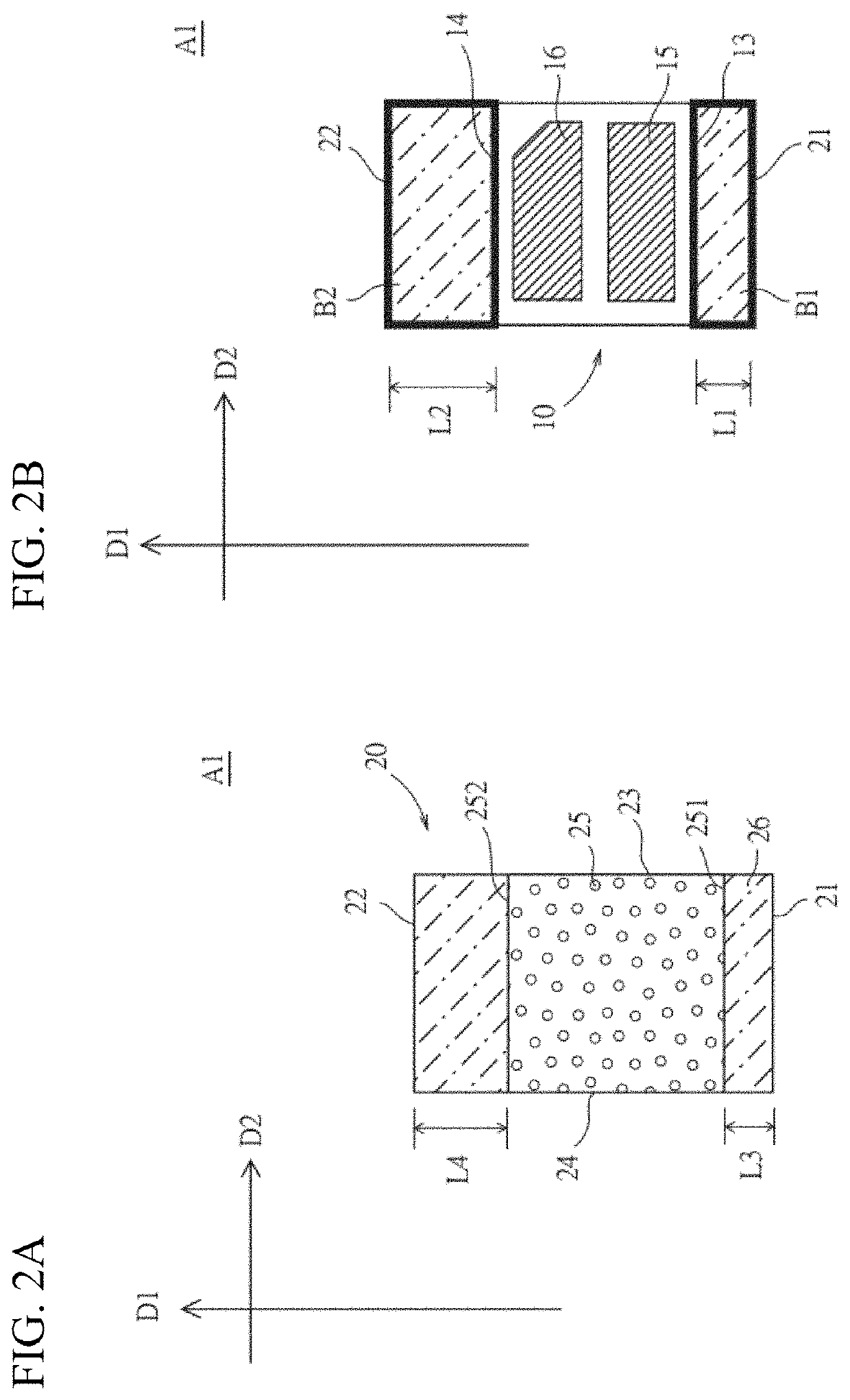
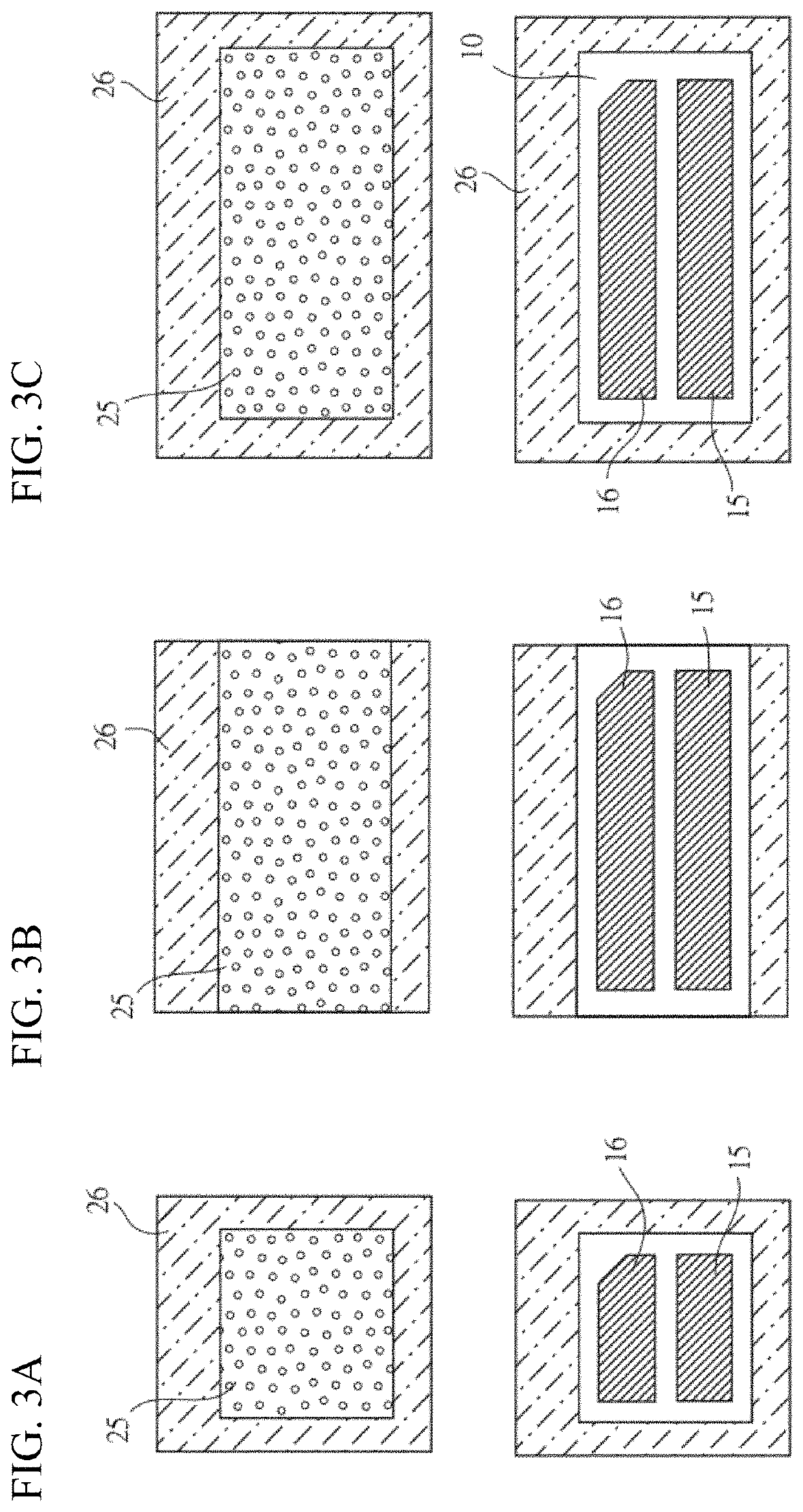
[0028]The following definitions apply to some of the technical aspects described with respect to some embodiments of the disclosure. These definitions may likewise be expanded upon herein.

[0029]As used herein, the singular terms “a,”“an,” and “the” may include plural referents unless the context clearly dictates otherwise. Thus, for example, reference to a layer can include multiple layers unless the context clearly dictates otherwise.

[0030]As used herein, the term “set” refers to a collection of one or more components. Thus, for example, a set of layers can include a single layer or multiple layers. Components of a set also can be referred to as members of the set. Components of a set can be the same or different. In some instances, components of a set can share one or more common characteristics.

[0031]As used herein, the term “adjacent” refers to being near or adjoining. Adjacent components can be spaced apart from one another or can be in actual or direct contact with ...


PUM

PropertyMeasurementUnit
light transmittanceaaaaaaaaaa

Abstract

A chip-scale packaging (CSP) light-emitting device (LED) is provided with an electrode polarity identifier, and includes a light-emitting semiconductor chip and a packaging structure. A first horizontal direction and a perpendicular second horizontal direction are specified on a semiconductor-chip-upper surface. The packaging structure covers the semiconductor-chip-upper surface, a first semiconductor-chip-side surface and a second semiconductor-chip-side surface of the light-emitting semiconductor chip, and includes a first package-side surface and a second package-side surface. A first region is between the first package-side surface and the first semiconductor-chip-side surface, and a second region is between the second package-side surface and the second semiconductor-chip-side surface, wherein an area of the first region is different from an area of the second region. An orientation of the electrode polarity of the CSP LED can be visually identified by recognizing the area difference of the first region and the second region.

Description

CROSS-REFERENCES TO RELATED APPLICATIONS[0001]This application claims the benefit of and priority to Taiwan Patent Application No. 107105605 filed on Feb. 14, 2018, and Chinese Patent Application No. 201810152166.3 filed on Feb. 14, 2018, the disclosures of which are incorporated herein by reference in their entirety.BACKGROUNDTechnical Field[0002]The present disclosure relates to a light-emitting device and a method of fabricating the same, and more particularly to a chip-scale packaging (CSP) light-emitting device (LED) with an electrode polarity identifier and a method of manufacturing the same.Description of the Related Art[0003]Light-emitting semiconductor chips are used as light sources to provide general illumination, backlight for liquid crystal display (LCD) panels, or as operation indicators for electronic devices, and light-emitting semiconductor chips are typically disposed in various package configurations (which may include phosphor materials inside packages) to become...

Claims


Application Information

Patent Timeline
Patent Type & Authority Patents(United States)
IPC IPC(8): H01L33/62H01L33/50H01L33/60
CPCH01L33/62H01L33/502H01L33/60H01L2933/0033H01L2933/0041H01L2933/0058H01L2933/0066H01L33/486H01L33/505
Inventor CHEN, CHIEH
Owner MAVEN OPTRONICS CO LTD
Why Eureka
Try Eureka