Near-infrared absorbing composition, optical structure, and camera module and electronic device comprising the same
a composition and near-infrared technology, applied in the direction of radiation controlled devices, instruments, other chemical processes, etc., to achieve the effect of improving near-infrared absorbance and reliability, and low visible absorban
- Summary
- Abstract
- Description
- Claims
- Application Information
AI Technical Summary
Benefits of technology
Problems solved by technology
Method used
Image
Examples
preparation example
[0226]5.6 g of 2-hydroxyethyl acryloyl phosphate (Sigma-Aldrich Corp.) and 5.2 g of copper(II) acetate [copper(II) acetate, Sigma-Aldrich Corp.] are dissolved in 30 g of acetone and then, reacted at room temperature for 5 hours, while stirred. Subsequently, the obtained reaction product is dripped into an excessive amount of a hexane solution to produce a precipitate, and the obtained precipitate is filtered and dried to obtain a copper complex represented by Chemical Formula 3-1.
[0227]
[0228]Separately, C0.33W1O3 particles having an average particle diameter of 80 nm as metal oxide particles (YMF-02, SUMITOMO Metal Mining Co., Ltd.) are prepared.
[0229]Separately, an amine-based compound represented by Chemical Formula 1-2 (Sigma-Aldrich Corp.) and a 3-functional polymerizable compound represented by Chemical Formula 2-1 (Sigma-Aldrich Corp.) are respectively prepared.
[0230]
[0231]Subsequently, 1 g of the copper complex and 13 mg of the metal oxide particles are put in 1 g of tetrahyd...
example 1
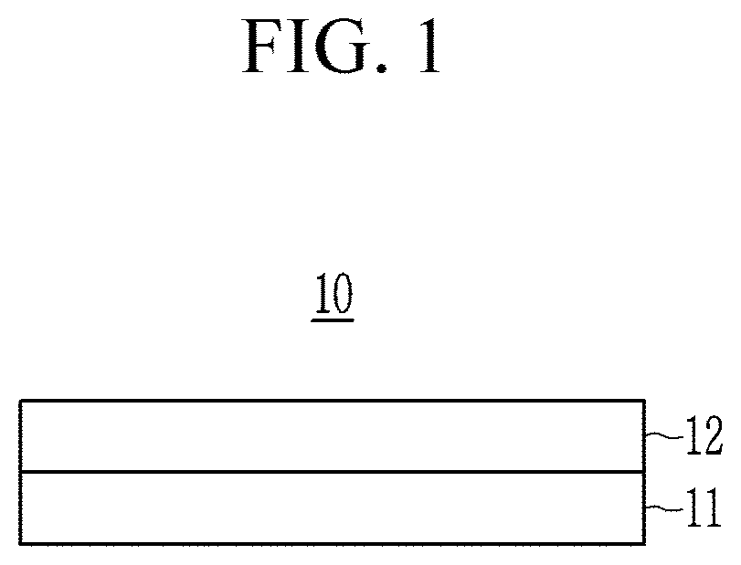
[0234]The near-infrared absorbing composition according to Preparation Example is bar-coated on an about 80 μm-thick cycloolefin polymer substrate film on which an about 2 μm-thick interface adhesive layer (CH-02, Samhwa Paints Industrial Co., Ltd.) is formed and specifically, right on the interface adhesive layer and then, dried at about 70° C. for 5 to 10 minutes to volatilize the solvent. Subsequently, the coated composition is photocured with a UV light dose of about 500 mJ to manufacture an optical structure according to Example 1. The cured first near-infrared absorption layer has a thickness of about 100 μm.
example 2
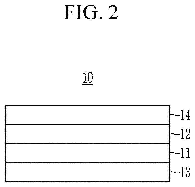
[0244]In Example 1, the first near-infrared absorption layer is cured, and then, an about 10 μm to 20 μm-thick cycloolefin polymer protective film is united thereon.
[0245]On the other hand, 0.03 g of a squarylium-based dye represented by Chemical Formula 4 and 1 g of a cycloolefin-based binder (TOPAS®) are added to and mixed with 10 mL of a chloroform solvent to prepare an organic near-infrared absorbing composition.
[0246]
[0247]Subsequently, the organic near-infrared absorbing composition is bar-coated to be about 20 μm-thick on the other side of the cycloolefin polymer substrate film on which the first near-infrared absorption layer is not formed and then, dried at about 70° C. for 5 to 10 minutes to manufacture an optical structure according to Example 2.
[0248]In the optical structure according to Example 2, the first near-infrared absorption layer including an inorganic material and the second near-infrared absorption layer including an organic material face each other while the ...
PUM
| Property | Measurement | Unit |
|---|---|---|
| wavelength region | aaaaa | aaaaa |
| wavelength region | aaaaa | aaaaa |
| wavelength | aaaaa | aaaaa |
Abstract
Description
Claims
Application Information


