Process for producing semiconductor device

a technology of semiconductor devices and processing equipment, applied in the direction of chemistry apparatus and processes, plasma technique, cleaning using liquids, etc., can solve the problems of inefficient conversion of plasma formed in high density into negative ions, difficult to achieve high efficiency, and decrease in plasma density

Inactive Publication Date: 2001-07-19
CANON KK
View PDF0 Cites 14 Cited by
  • Summary
  • Abstract
  • Description
  • Claims
  • Application Information

AI Technical Summary

Problems solved by technology

The above two methods, however, have had the following problems.
However, in the case of etching carried out by predominantly using negative ions, it is difficult to attain a high efficiency because the negative ions are formed only in the half of the processing time.
ii) In the method where plasma is guided spatially downstream to lower a plasma temperature to form negative ions, the recombination of plasma at vacuum vessel walls causes an abrupt decrease in plasma density itself, and hence the plasma formed in a high density can not efficiently be converted into negative ions.

Method used


Image

  • Process for producing semiconductor device
  • Process for producing semiconductor device
  • Process for producing semiconductor device

Examples


example 2

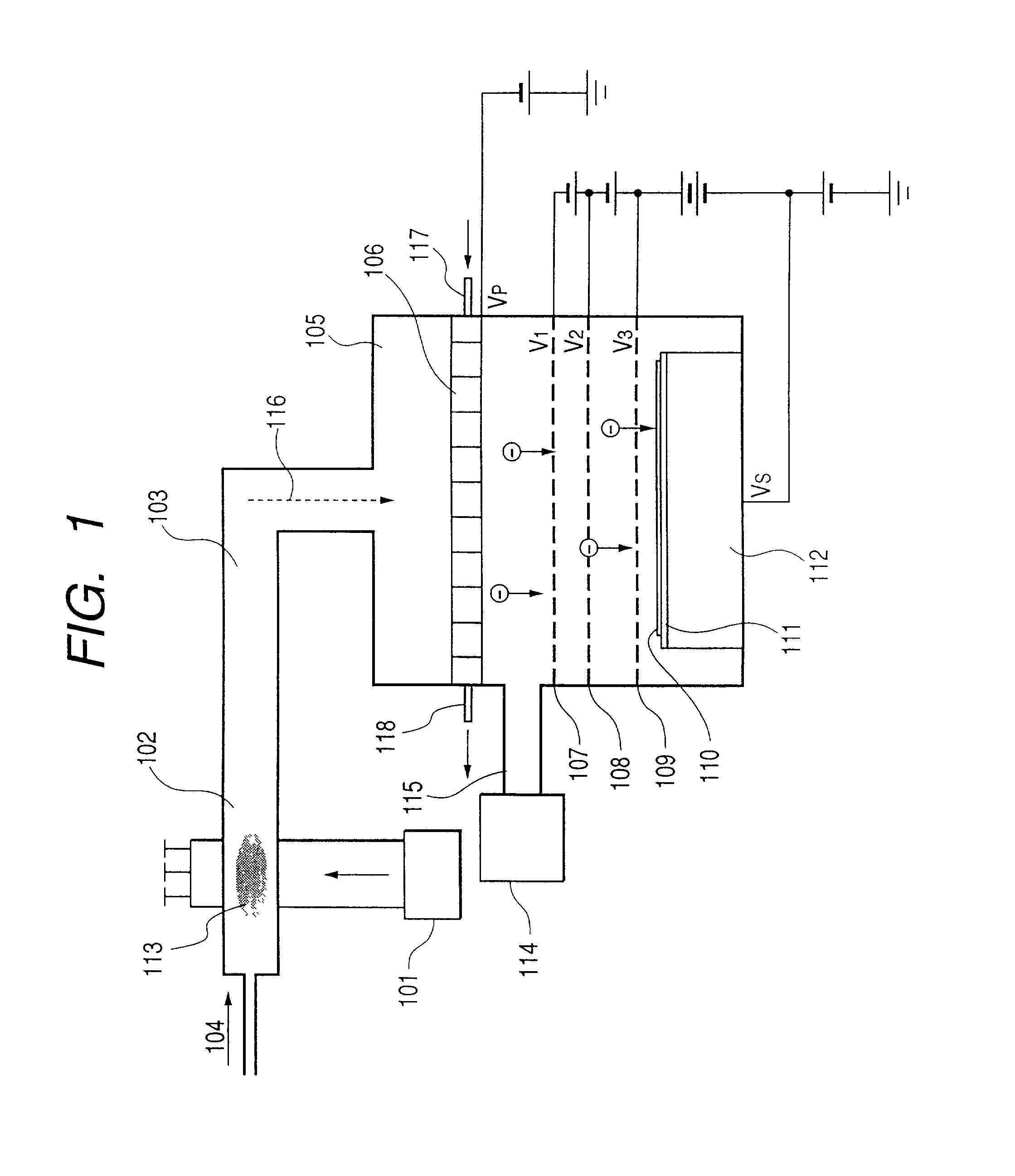
[0062] In the present Example, the apparatus shown in FIG. 1 was used in a cleaning process carried out before a film for upper-layer metal wiring is formed, in a via hole forming process for connecting different wiring layers of multi-layer wiring in semiconductor fabrication processes, and whether or not any charge-up damage occurred was examined.

[0063] Native oxide films or crystal defects brought in by ion bombardment at the time of etching remain at the bottoms of via holes formed above the silicon substrate surface. Hence, if second-layer metal wiring is formed in the state the via holes are left as they are, the native oxide films or crystal defects cause increase of the resistance of the via holes to bring about circuit retardation or wiring faulty conduction. Accordingly, these residual matter must be removed by cleaning or the like. At present, methods making use of plasma are widely and commonly used. The problem of these methods is the phenomenon of charge-up caused by p...

example 3

[0071] In the present Example, an instance is described where the apparatus shown in FIG. 3 was used and the second gas for cooling the plasma was fed in the form of neutral active particles.

[0072] By using the above apparatus, the etching rate of the polycrystalline silicon film was measured in the same manner as in Example 1. In this case, the wafer having a silicon oxide film on which a non-doped polycrystalline silicon film was deposited was used as the article 310 to be processed.

[0073] First, the article 310 to be processed was placed on the supporting stand 312 of the apparatus shown in FIG. 3. Thereafter, the plasma generating space 302 and the inside of the processing chamber 305 were evacuated via an exhaust means until they came to have a degree of vacuum of 5.times.10.sup.-6 Torr. Thereafter, 100 sccm of Cl.sub.2 gas was fed into the plasma generating space 302 through the first-gas inlet 304, and a throttle valve (not shown) installed to the exhaust means was adjusted t...


PUM

PropertyMeasurementUnit
incident energyaaaaaaaaaa
voltageaaaaaaaaaa
voltageaaaaaaaaaa

Abstract

A plasma processing apparatus having a vacuum vessel and a supporting means for supporting a processing target in the vacuum vessel, the apparatus comprising means for introducing a gas into a plasma generating space, means for feeding electric energy to the gas in the plasma generating space to generate a plasma, a metal member for forming negative ions which is provided on the downstream side of the plasma generating space in such a way that it comes into contact with particles of the plasma, and means for feeding the negative ions to the processing target. Utilizing the electric charge exchange reaction between plasma particles and metal surfaces, negative ions can be formed continuously and in a high density and also the negative ions can be made incident on a processing target to make ashing, etching or cleaning of the processing target to remove unwanted matter therefrom, so that a high processing rate and less charge-up damage can be achieved.

Description

[0001] 1. Field of the Invention[0002] This invention relates to a plasma processing apparatus and a processing method making use of the same. More particularly, it relates to a plasma processing apparatus by which negative ions can be generated in a large quantity and also the negative ions can be made incident on an article to be processed to etch or clean the article to remove unwanted matter therefrom, and a processing method making use of the same. This plasma processing apparatus is preferably used in processes for producing semiconductor devices such as LSIs, optical devices such as optical disks and waveguides, and magnetic devices such as magnetic disks.[0003] 2. Related Background Art[0004] In general, it is said to be important to lower a plasma temperature in order to form negative ions in a plasma processing apparatus. The relationship between the plasma temperature and the negative ion formation can be known from the probability of attachment of electrons to particles ...

Claims


Application Information

Patent Timeline
Patent Type & Authority Applications(United States)
IPC IPC(8): H01L21/302C23F4/00H01J37/32H01L21/3065H05H1/46
CPCH01J37/32357H01J37/32422
Inventor KITAGAWA, HIDEO
Owner CANON KK
Why Eureka
Try Eureka