Data processing method by programmable logic device, programmable logic device, information processing system and method of reconfiguring circuit in programmable logic

a data processing and programmable logic technology, applied in the field of data processing methods by programmable logic devices, programmable logic devices, information processing systems and methods of reconfiguring circuits in programmable logic, can solve the problems of slow software processing speed, large processor size, and short flexibility of hardware processing

Inactive Publication Date: 2001-07-26
FUJIFILM BUSINESS INNOVATION CORP
View PDF5 Cites 80 Cited by
  • Summary
  • Abstract
  • Description
  • Claims
  • Application Information

AI Technical Summary

Benefits of technology

[0213] Also, to compare the effect of the invention with that of prior art, a device equivalent to XCV50 based upon multicontext technique provided with three configuration memories (559,232 bits'3 1677,696 bits) corresponding to each processing of DCT, quantization and entropy coding shall also be supposed.
[0214] An image to be processed is an image including 1024 pixels.times.1024 pixels.times.8 bits. As a processing unit is an 8.times.8 pixel block (8 pixels.times.8 pixels.times.8 bits=512 bits / block), the number of blocks of input data is 16,384 acquired by calculating (1024 pixels.times.1024 pixels) / (8 pixels.times.8 pixels).
[0215] As the number of digits of data is increased during processing though the precision of input data is 8 bits, the data cache 53 or the data cache circuit 524 shall store data in units of 16 bits. At this time, the maximum value of the number k of blocks of data which the data cache 53 or the data cache circuit 524 can store is 546.125 acquired by calculating 559,232 bits / (8 pixels.times.8 pixels.times.16 bits). In this concrete example, k=512.
[0216] (Time Required For Reconfiguration in Case Conventional Type Programmable Logic Device is Used)
[0217] First, circuit configuration time in conventional type reconfigurable computing using XCV50 which can be dynamically partially reconfigured will be estimated.
[0218] As already described, one block of data is processed by reading circuit information three times and the succeeding data processing and all input data is processed by repeating this cycle by the number N of blocks of the input data. Therefore, if time required for reading three circuit information pieces is respectively Tcd1, Tcd2 and Tcd3, circuit configuration time T (conventional type) required for processing N blocks of data is as follows.T (conventional type)=(Tcd1+Tcd2+Tcd3).times.N

Problems solved by technology

On the other hand, as overhead for fetching an instruction from a memory storing a program and decoding it and for writing the result of an execution to the memory is required, software processing is slower in processing speed, compared with hardware processing operated at the same clock frequency.
Also, there is a defect that as a main storage for storing a program and a secondary storage are required, a processor is large-sized.
On the other hand, as the connection of circuits once produced cannot be varied, hardware processing is short of flexibility, compared with software processing, plural dedicated processing circuits are required to process data of plural systems and a circuit once produced cannot correspond to a new system.
Hardware processing using a programmable logic device to solve the defect described above that hardware processing is short of flexibility is recently attracting attention.
However, in the case of the conventional type example 1, there is a problem that time for writing circuit information to a configuration memory of the programmable logic device of the client computer CL from the application server SB is long depending upon the scale of the circuit information (an extension code) to be written to the configuration memory of the programmable logic device and even if high-speed processing is implemented using the extended hardware which is a dedicated hardware processing circuit, the whole processing time including circuit reconfiguration time is longer than processing time by software.
As the load capacity of the circuit element is increased when the scale of the circuit is enlarged, a problem is caused that the performance of the circuit is deteriorated and the power consumption is increased.
Also, when the scale of the circuit is enlarged, a problem is caused that the manufacturing cost of the programmable logic device is increased.
As described above, in the case of a reconfiguration method using the conventional type programmable logic device, plural circuits are required to be sequentially repeatedly reconfigured per block, the frequency of reconfiguration is required by (the number of blocks.times.the number of circuits) and therefore, there is a problem that total processing time is long.

Method used


Image

  • Data processing method by programmable logic device, programmable logic device, information processing system and method of reconfiguring circuit in programmable logic
  • Data processing method by programmable logic device, programmable logic device, information processing system and method of reconfiguring circuit in programmable logic
  • Data processing method by programmable logic device, programmable logic device, information processing system and method of reconfiguring circuit in programmable logic

Examples


first embodiment

[0155] -First Embodiment-

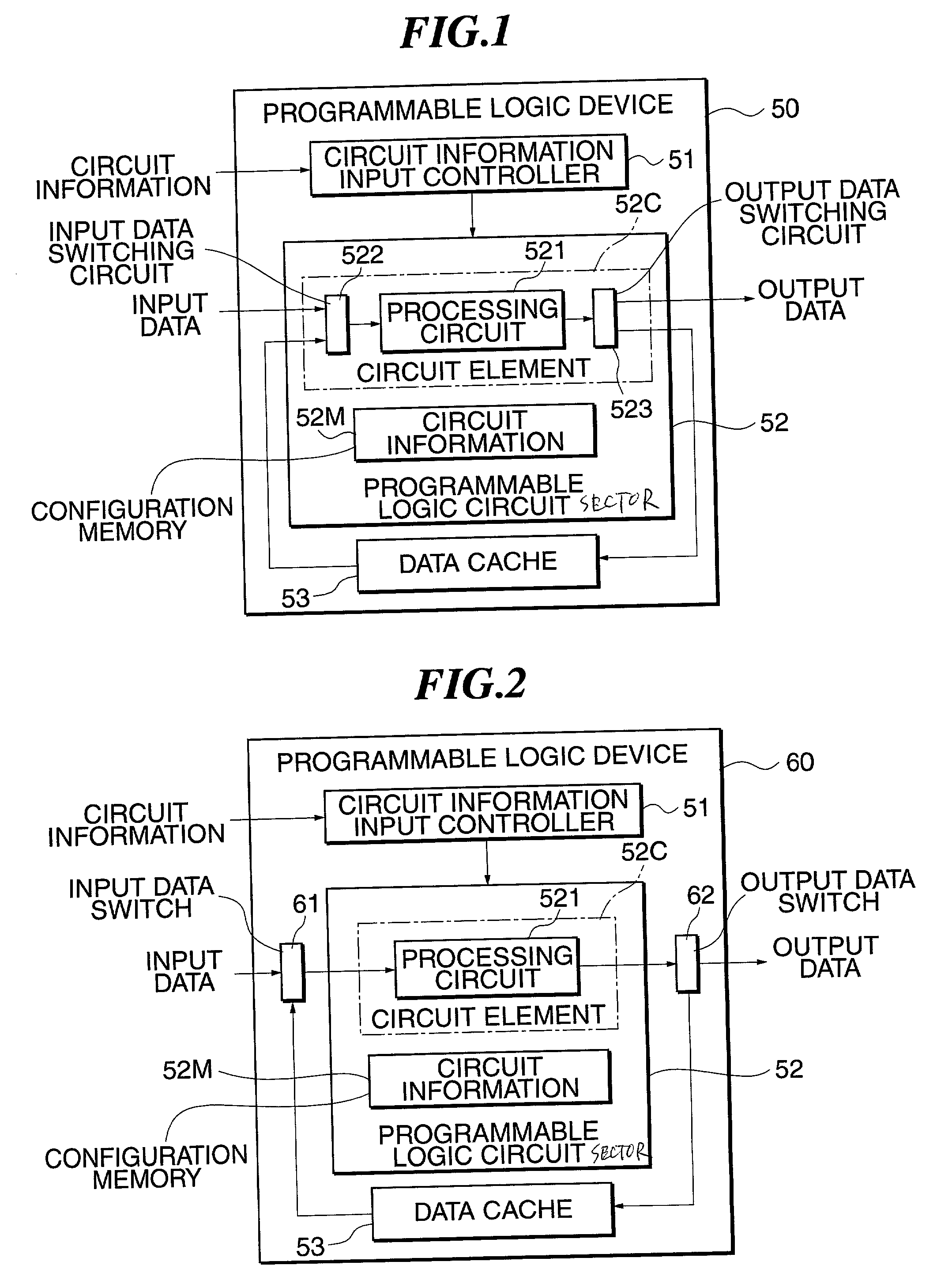
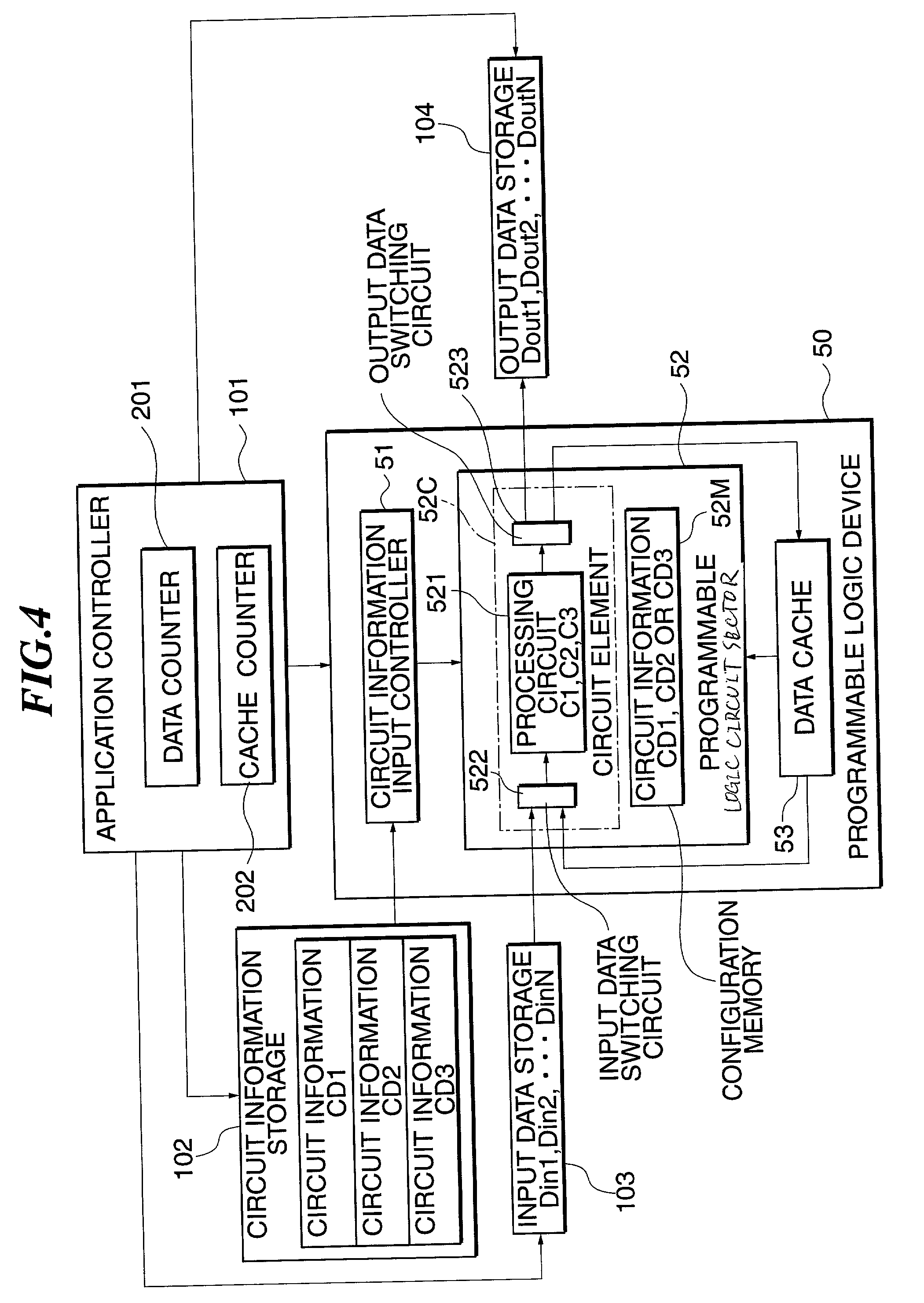
[0156] In an embodiment of an information processing system and a data processing method according to the invention, data processing for sequentially processing input data in units of block by plural circuits is executed by the information processing system using any of the programmable logic device 50 provided with the first structure, the programmable logic device 60 provided with the second structure and the programmable logic device 70 provided with the third structure as described in the item of the problems to be solved by the invention.

[0157] Data processing for sequentially processing N blocks (N sets) of input data Din1, Din2, - - - , DinN by processing circuits C1, C2 and C3 configured by sequentially reading circuit information CD1, CD2 and CD3 in a configuration memory 52M of a programmable logic circuit sector 52 via a circuit information input controller 51 and acquiring N blocks (N sets) of output data Duot1, Dout2, - - - , DoutN will be descr...


PUM


Abstract

To provide a method of implementing cache logic technique in which total data processing time can be reduced, input data divided into block is sequentially processed in units of block in plural circuits using a programmable logic device provided with a circuit information input controller, a programmable logic circuit sector and a data cache. The plural circuits are sequentially reconfigured in the programmable logic device and execute processing per plural blocks which can be stored in the data cache. Intermediate data in units of plural blocks is stored in the data cache to be input data to a reconfigured circuit and intermediate data as the result of the processing by the reconfigured circuit is overwritten to the data cache. When the processing of the plural circuits is finished, the result of the processing is output to an external device without being stored in the data cache.

Description

[0001] 1. Field of the Invention[0002] The present invention relates to an information processing system that enables a part of processing by an application program for example to be processed using a programmable logic device of which the circuit can reconfigured, a data processing method in the information processing system and the programmable logic device used for the information processing system. Particularly, the present invention relates to a method of reducing processing time including time required for the reconfiguration of the programmable logic device.[0003] 2. Description of the Related Art[0004] In the field of a digital device, a programmable logic device (PLD) such as a field programmable gate array (FPGA) has been used for a prototype device before an application specific integrated circuit (ASIC) is produced or for an alternative device of ASIC requiring a long production term of several weeks or months. Also, recently, a programmable logic device is used for chan...

Claims


Application Information

Patent Timeline
Patent Type & Authority Applications(United States)
IPC IPC(8): G06F9/30G06F9/06G06F9/32G06F9/38G06F15/78H03K19/173
CPCG06F9/325G06F9/3885G06F9/3897G06F15/7867
Inventor NISHIHARA, YOSHIOSATO, YOSHIHIDEYAMADA, NORIKAZUSATONAGA, TETSUICHI
Owner FUJIFILM BUSINESS INNOVATION CORP
Why Eureka
Try Eureka