
Thin film transistor with sub-gates and schottky source/drain and a manufacturing method of the same

a technology manufacturing methods, applied in the field of thin film transistors, can solve the problems of not being able to operate in bi-channel mode, not being able to advantageously lower the process temperature, etc., and achieve the effects of reducing process complexity and cost, lowering process temperature, and reducing off-state leakag

Inactive Publication Date: 2002-01-24
S M SZE +1
View PDF0 Cites 37 Cited by
  • Summary
  • Abstract
  • Description
  • Claims
  • Application Information

AI Technical Summary

Benefits of technology

[0011] Another object of the present invention is to apply voltage to the sub-gate to induce the formation of an electrical junction, which takes place the conventional source / drain extension; which results in the reduction of cut-off leakage.
[0047] Subsequently, a second conductive layer is deposited on the gate dielectric layer 35 and the second insulation layer 33. The second conductive layer is then defined and etched by lithography to form an island-shaped main gate layer 36, shown in FIG. 3g. Two ends of the island-shaped main gate layer overlap respectively with the proportional areas on top of the two island-shaped sub-gate layer 31. The second conductive layer is selected from metal layer or highly doped polysilicon formed by PVD or CVD. If the island-shaped main gate layer 36 is a metal gate, a dielectric layer must be deposited on it, so that the gate becomes a stacking layers of dielectric layer / metal. The dielectric layer is silicon oxide or silicon nitride, with a thickness of 20 to 100 nm. The dielectric layer is used to protect the metal layer underneath it from damage caused by following wet etching.
[0087] Next, a first conductive layer is formed on the gate dielectric layer 82, which is then etched by lithography to an island-shaped main gate 83, shown in FIG. 8c. The first conductive layer is of a metal layer formed by PVD or CVD or highly doped polysilicon. If the island-shaped main gate layer 83 is a metal gate, a dielectric layer must be deposited on it so that the gate becomes a dielectric layer / metal stacking layer. The dielectric layer is silicon oxide or silicon nitride with a thickness between 20 and 100 nm. The dielectric layer is used to protect the metal layer underneath it from damage by the follow-up wet etching.
[0105] Next, a first conductive layer is formed on the gate dielectric layer 102, which is then etched by lithography to an island-shaped main gate 103, shown in FIG. 10c. The first conductive layer is of a metal layer formed by PVD or CVD or highly doped polysilicon. If the island-shaped main gate layer 103 is a metal gate, a dielectric layer must be deposited on it so that the gate becomes a dielectric layer / metal stacking layer. The dielectric layer is silicon oxide or silicon nitride with a thickness between 20 and 100 nm. The dielectric layer is used to protect the metal layer underneath it from damage by the following wet etching.
[0149] From the above, it is not necessary to carry out implant doping and the following annealing steps in this invention. Therefore, the complexity and costs of the process are decreased. This is also advantageous in lowering the process temperature. Moreover, by adjusting the biased voltage of V.sub.g-sub, a single device is able to operate in both n type and p type channels.
[0150] This invention utilizes the application of voltage to the sub-gate to induce electrical junction, which takes the place of the conventional source / drain extensions. As a result, off-state leakage is decreased.

Problems solved by technology

Because implant doping and the following annealing must be carried out, it is not advantageous to lower the process temperature.
Depending on the type of dopant in the source / drain, the operation mode of a thin film transistor is restricted as n type or p type, which does not allow for bi-channel operation.

Method used


Image

  • Thin film transistor with sub-gates and schottky source/drain and a manufacturing method of the same
  • Thin film transistor with sub-gates and schottky source/drain and a manufacturing method of the same
  • Thin film transistor with sub-gates and schottky source/drain and a manufacturing method of the same

Examples


first embodiment

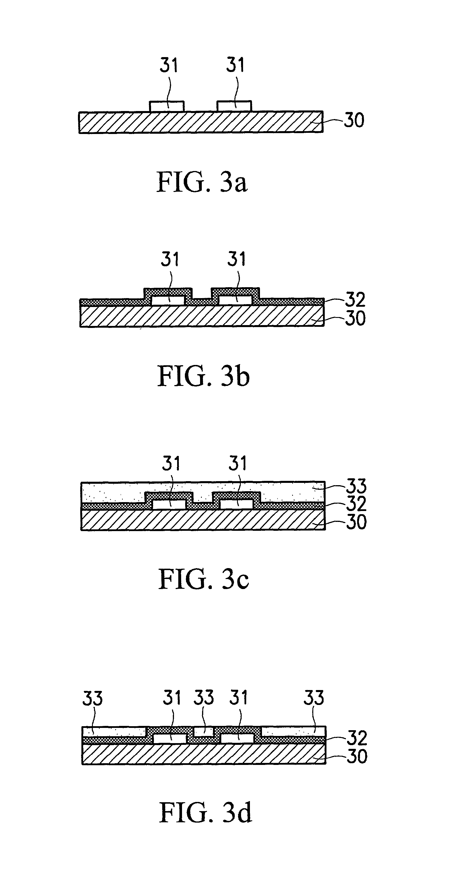
[0040] Refer to FIGS. 3a.about.3i, which illustrate the cross-sectional diagrams of the process according to the invention.

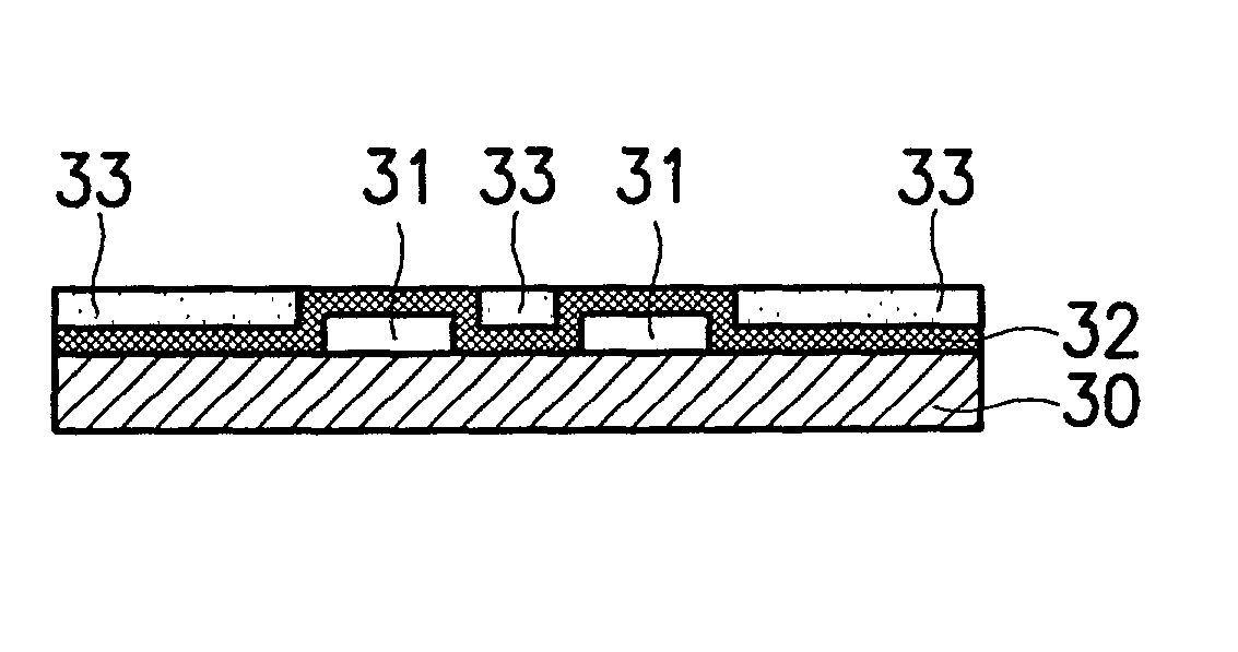
[0041] First, an insulation substrate 30 is provided; it is SiO.sub.2 or quartz. A first conductive layer is then formed on the insulation substrate 30. The first conductive layer is then defined and etched by lithography shown in FIG. 3a, to form two island-shaped sub-gate layers 31 on the insulation substrate 30. The first conductive layer is of a material selected from metal or highly doped polysilicon. The thickness is 30.about.200 nm.

[0042] A first insulation layer 32 is conformally formed on the island-shaped sub-gate layers 31 and the insulation substrate 30, shown in FIG. 3b. The first insulator 32 is silicon nitride layer formed by CVD with a thickness from 30 to 200 nm.

[0043] A second insulation layer 33 is formed on the first insulation layer 32, followed by chemical mechanical polishing (CMP) to planarize the surface, shown in FIG. 3c. The second ins...

fourth embodiment

[0066] Refer to FIGS. 6a.about.6h, which illustrate the cross-sectional diagrams of the process of fourth embodiment in this invention.

[0067] First, an insulation substrate 60, of, for example, SiO2 or quartz, is provided. Next, a thin semiconductor layer is formed on the insulation substrate 60. The semiconductor layer is then defined and etched to form an island-shaped semiconductor layer 61 on the insulation substrate, shown in FIG. 6a. The thickness of the thin semiconductor is between 10 and 200 nm. The material is selected from single silicon, amorphous silicon or polysilicon.

[0068] A first insulation layer 62, a first conductive layer 63 and a second insulation layer 64 are sequentially formed on the island-shaped semiconductor 61 and the insulation substrate 60, shown in FIG. 6b. The first insulation layer 62 is a silicon nitride layer formed by CVD with a thickness between 10 and 100 nm. The first conductive layer 63 is selected from a metal layer or highly doped polysilico...

sixth embodiment

[0084] Refer to FIGS. 8a.about.8g, which illustrate the cross-sectional diagrams of the process of sixth embodiment in this invention.

[0085] First, an insulation substrate 80, of, for example, SiO2 or quartz is provided. Next, a thin semiconductor layer is formed on the insulation substrate 80. The semiconductor layer is then defined and etched to form an island-shaped semiconductor layer 81 on the insulation substrate, shown in FIG. 8a. The thickness of the thin semiconductor layer is between 10 and 200 nm. The material is selected from single silicon, amorphous silicon or polysilicon.

[0086] A gate dielectric layer 82 is formed on the surface of the island-shaped semiconductor 81 by thermal oxidation or CVD, shown in FIG. 8b. The gate dielectric layer 82 is oxide layer in this embodiment.

[0087] Next, a first conductive layer is formed on the gate dielectric layer 82, which is then etched by lithography to an island-shaped main gate 83, shown in FIG. 8c. The first conductive layer i...


PUM


Abstract

The present invention discloses a thin film transistor with sub-gates and Schottky source / drain and a method of manufacturing the same. Doping of source / drain, and the following annealing steps used conventionally are omitted and the complexity of process and process costs are reduced. The temperature of the process is also decreased. A thin film transistor with sub-gates and Schottky source / drain of the invention is able to operate in both the n type and p type channel modes on the same transistor element depending on the biased voltage of the sub-gate. Moreover, an electric junction is formed by induction, using bias voltage applied on the sub-gate, which takes the place of the conventional source / drain extensions. Consequently, the off-state leakage current is reduced.

Description

[0001] 1. Field of the Invention[0002] The present invention relates to a thin film transistor and a manufacturing method of the same, and more particularly, to a thin film transistor with sub-gates and Schottky source / drain and a manufacturing method of the same.[0003] 2. Description of the Prior Art[0004] FIG. 1 shows the structural diagram of a conventional thin film transistor. In FIG. 1, 10 represents a glass or quartz substrate; 12 denotes a semiconductor layer, eg. polysilicon; 14 represents a doping area on the semiconductor 12, which serves as source / drain of the thin film transistor 1; and 16 represents gate oxide layer; and 18 represents gate.[0005] The shortcomings of the conventional thin film transistor 1 are:[0006] Because implant doping and the following annealing must be carried out, it is not advantageous to lower the process temperature.[0007] Depending on the type of dopant in the source / drain, the operation mode of a thin film transistor is restricted as n type ...

Claims


Application Information

Patent Timeline
IPC IPC(8): H01L21/20H01L21/28H01L21/336H01L29/45H01L29/47H01L29/786H01L29/872
CPCH01L29/458H01L29/78609H01L29/78636H01L29/78645
Inventor LIN, HORNG-CHIHTSAI, MING-SHIHHUANG, TIAO-YUAN
Owner S M SZE
Learn More