Active photonic crystal waveguide device and method

Inactive Publication Date: 2002-02-21
CORNING INC
View PDF0 Cites 98 Cited by
  • Summary
  • Abstract
  • Description
  • Claims
  • Application Information

AI Technical Summary

Benefits of technology

0023] Another aspect of the present invention relates to a method for controlling an optical signal including providing a device including a planar photonic crystal structure having a defect waveguide, an upper clad region continuous with the top surface of the defect waveguide, and a lower clad region continuous with the bottom surface of the defect waveguide, wherein at least one of the upper clad region or the lower clad region is a controllable region having a controllable optical property sufficient to modify the optical signal; launching the optical signal into the defect waveguide; and controlling the optical property of at least one of the upper clad region or the lower clad region so as to effect a change in the propagation of the optical signal in the defect waveguide.
0024] The device of the present invention results in a number of advantages. Active planar photonic crystal defect waveguide devices may be designed and f

Problems solved by technology

While the defect in the above example is a constructed from a row of missing air-filled columns, other defect structures are possible.
Solution of the full vector Maxwell equations required, as the simpler scalar approximation gives incorrect results due to the large dielectric/air index.
Active photonic crystal materials and device

Method used


Image

  • Active photonic crystal waveguide device and method
  • Active photonic crystal waveguide device and method
  • Active photonic crystal waveguide device and method

Examples


Embodiment Construction

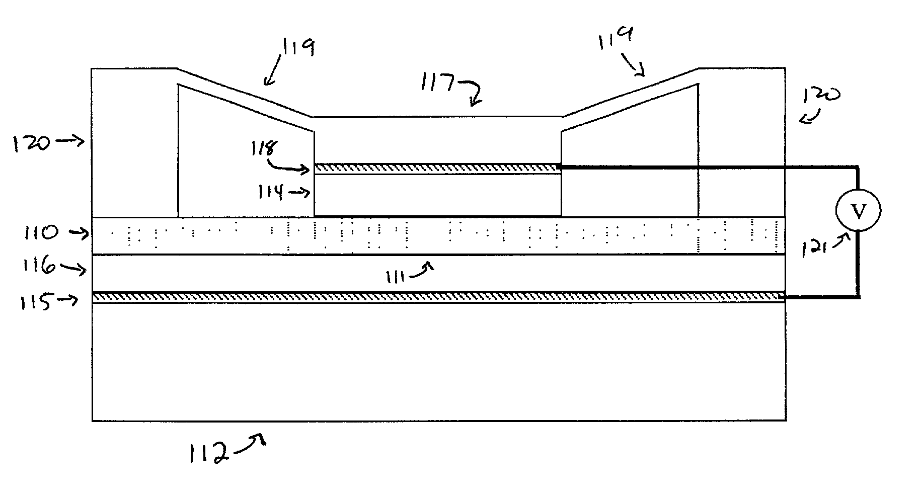
[0055] Reference will now be made in detail to the present preferred embodiments of the invention, examples of which are illustrated in the accompanying drawings. Wherever possible, the same reference numerals will be used throughout the drawings to refer to the same or like parts.

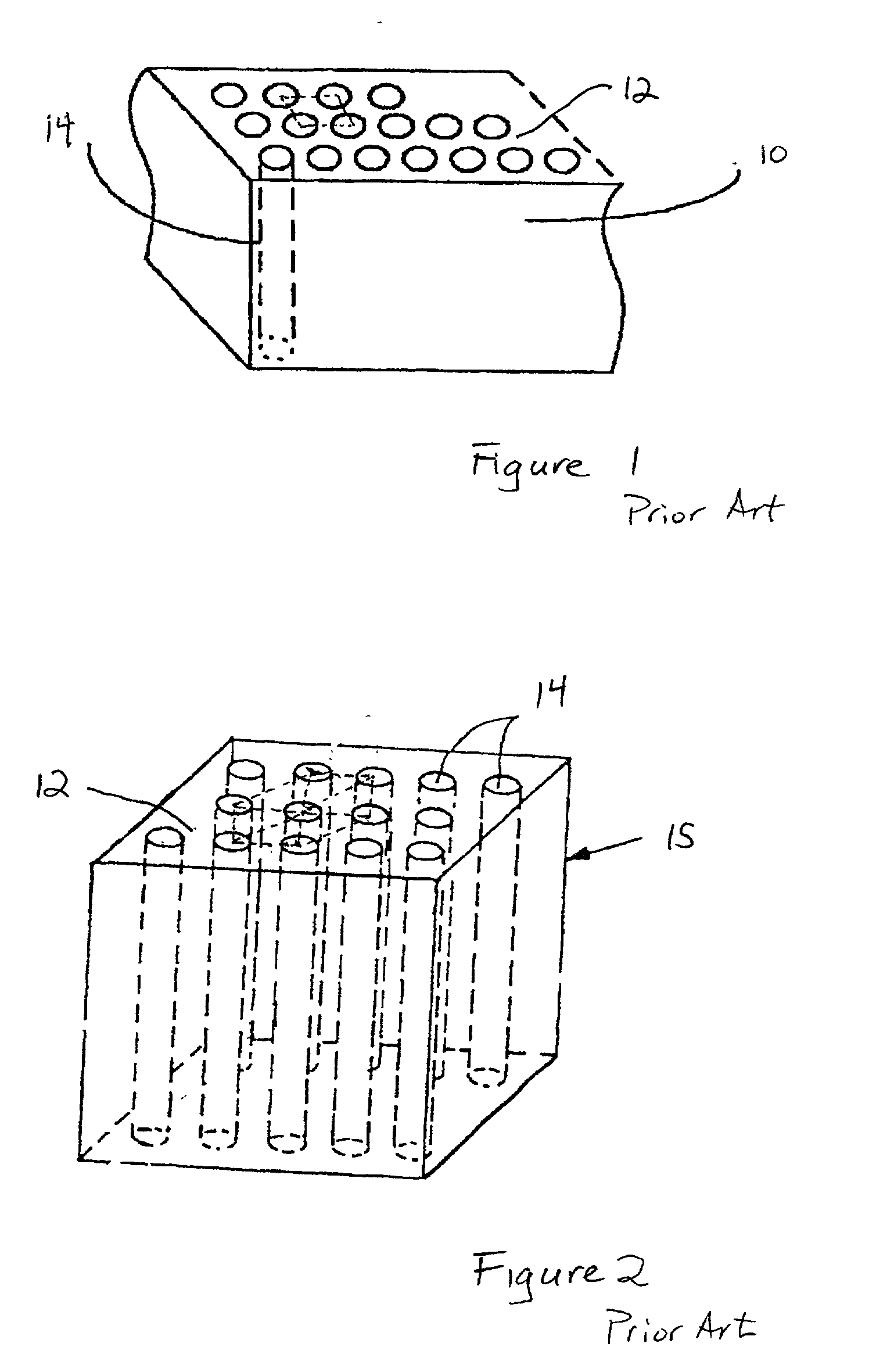
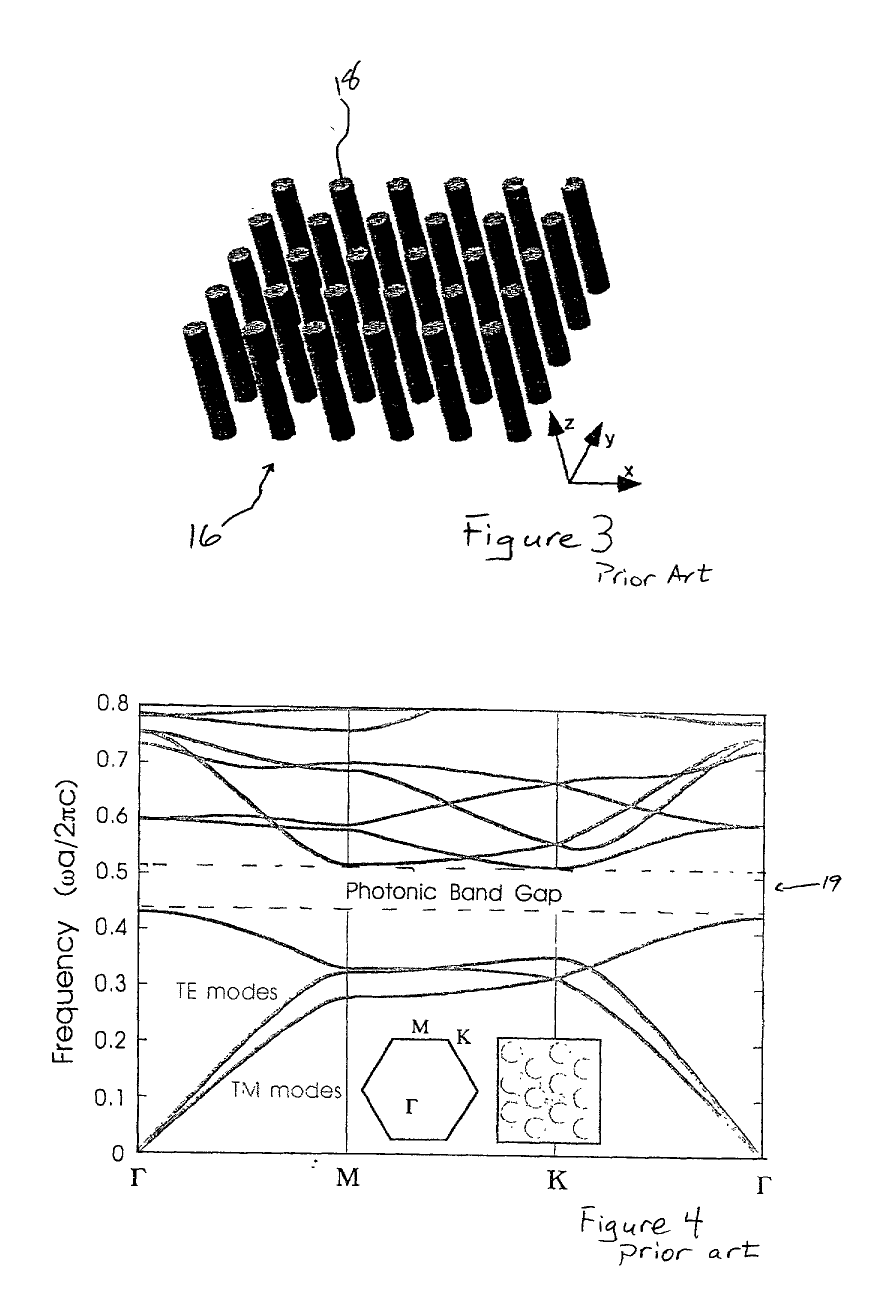
[0056] Referring now to FIG. 14, a perspective view of a general planar photonic crystal defect waveguide device is shown. The device consists of a thin slab 100 of planar photonic crystal material, having, for example, air-filled columns 14 disposed in a hexagonal array in a bulk material 12. Alternatively, the geometry of the array may be square, triangular, rectangular, or more complex, depending on the desired in-plane photonic band gap. The bulk material may be any material transparent to the wavelengths of the optical signal. For example, the planar photonic crystal bulk material may be doped silica, undoped silica, silicon, a polymeric organic material, a organic / inorganic hybrid material, an inorga...


PUM


Abstract

An active photonic crystal device for controlling an optical signal is disclosed. The device includes a planar photonic crystal with a defect waveguide bounded on the top and bottom by an upper cladding region and a lower cladding region. An optical signal propagating in the defect waveguide is confined in the plane of the photonic crystal by the photonic bandgap, and in the direction normal to the photonic crystal by the upper clad region and the lower clad region. The propagation of the optical signal in the defect waveguide is controlled by varying the optical properties at least one of the upper clad region or the lower clad region. The variation of the optical properties of the controllable regions may be achieved using a thermo-optic effect, an electro-optic effect, a stress-optic effect, or a mechano-optic effect, or by moving a material into or out of the controllable region.

Description

CROSS-REFERENCE TO RELATED APPLICATIONS[0001] This application claims priority under 35 U.S.C .sctn. 119(e) to U.S. Provisional Application No. 60 / 225,488, filed Aug. 15, 2000, which is incorporated herein by reference; and U.S. Provisional Application No. 60 / 269,163, filed Feb. 15, 2001, which is incorporated herein by reference.[0002] BACKGROUND OF THE INVENTION[0003] 1. Field of the Invention[0004] The present invention relates generally to an optical waveguide structure for an optical communication system, and particularly to a planar photonic crystal waveguide for implementing a variety of optical functions in an optical communication system.[0005] 2. Technical Background[0006] Photonic crystals are periodic optical materials. The characteristic defining a photonic crystal structure is the periodic arrangement of dielectric or metallic elements along one or more axes. Thus, photonic crystals can be one-, two-, and three-dimensional. Most commonly, photonic crystals are formed f...

Claims


Application Information

Patent Timeline
IPC IPC(8): G02B6/122G02B6/125G02B6/35G02F1/01
CPCB82Y20/00G02B6/1225G02B6/125G02B6/3538G02B6/3546G02F2202/32G02B6/3584G02B6/3596G02F1/01G02F1/011G02F1/0147G02B6/3582G02F1/21
Inventor ALLAN, DOUGLAS C.COTTRVERTE, JEAN-CHARLES J.C.KUCHINSKY, SERGEY A.RENVAZE, CHRISTOPHE F.P.
Owner CORNING INC
Why Eureka
Try Eureka