Soft-switched full-bridge converters

a converter and full-bridge technology, applied in the direction of electric variable regulation, process and machine control, instruments, etc., can solve the problems of increasing component stresses, restricting the maximum frequency of operation of "hard-switched" converters, and affecting the operation of conventional pulse-width modulated converters

Inactive Publication Date: 2002-04-18
DELTA ELECTRONICS INC
View PDF0 Cites 18 Cited by
  • Summary
  • Abstract
  • Description
  • Claims
  • Application Information

AI Technical Summary

Benefits of technology

[0016] Since the energy used to create the ZVS condition at light loads is not stored in the leakage inductances of the transformer, the transformer's leakage inductances can be minimized, which also minimizes the duty-cycle loss on the secondary side of the transformer. As a result, the converters of this invention can operate with the largest duty cycle possible, thus minimizing both the conduction loss of the primary switches and voltage stress on the components on the secondary side of the transformer, which improves the conversion efficiency. Moreover, because of the minimized leakage inductances, the secondary-side parasitic ringing caused by a resonance between the leakage inductances and the junction capacitance of the rectifier is also minimized so that the power dissipation of a snubber circuit usually required to damp the ringing is also reduced.

Problems solved by technology

The major factors hindering the operation of conventional ("hard-switched") pulse-width-modulated (PWM) converters at higher switching frequencies are circuit parasitics such as semiconductor junction capacitances, transformer leakage inductances, and rectifier reverse recovery.
Generally, these parasites introduce additional switching losses and increase component stresses, and, consequently, limit the maximum frequency of operation of "hard-switched" converters.
In addition, the majority of resonant topologies need to circulate a significant amount of energy to create ZCS or ZVS conditions, which increases conduction losses.
This strong trade-off between the switching-loss savings and increased conduction losses may result in a lower efficiency and / or larger size of a high-frequency resonant-type converter compared to its PWM counterpart operating at a lower frequency.
In addition, variable frequency of operation is often perceived as a disadvantage of resonant converters.
As a result, although resonant converters are used in a number of niche applications such as those with pronounced parasitics, the resonant technique has never gain a wide acceptance in the power-supply industry in high-frequency high-power-density applications.
Since leakage inductance L.sub.LK is small, the energy stored in L.sub.LK is also small so that ZVS of Q.sub.1 and Q.sub.2 is hard to achieve even at relatively high output currents.
However, a large external inductance also stores an extremely high energy at the full load, which produces a relatively large circulating energy that adversely affects the stress of the semiconductor components, as well as the conversion efficiency.
This extended commutation time results in a loss of duty cycle on the secondary of the transformer, which further decreases the conversion efficiency.
With a smaller transformer's turns ratio, the reflected output current into the primary is increased, which increases the primary-side conduction losses.
Moreover, since a smaller turns ratio of the transformer increases the voltage stress on the secondary-side rectifiers, the rectifiers with a higher voltage rating that typically have higher conduction losses may be required.
Finally, it should be noted that one of the major limitations of the circuit in FIG. 1(a) is a severe parasitic ringing at the secondary of the transformer during the turn-off of a rectifier.
To control the ringing, a heavy snubber circuit needs to be used on the secondary side, which may significantly lower the conversion efficiency of the circuit.
However, even with the modifications, the performance of these converters is far from optimal.

Method used


Image

  • Soft-switched full-bridge converters
  • Soft-switched full-bridge converters
  • Soft-switched full-bridge converters

Examples


Embodiment Construction

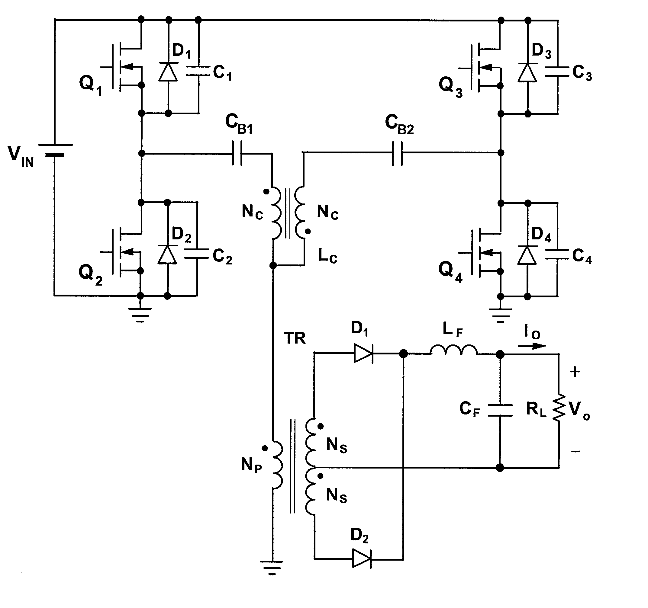
[0037] FIG. 3 shows one of the generalized embodiments of the isolated, phase-shift-controlled FB ZVS-PWM converter of this invention. The circuit in FIG. 3, employs two transformers TX and TY, which have their respective secondary outputs connected to two output circuits X and Y. Generally, in the dc / dc implementations of the converter in FIG. 3, each output circuit X and Y includes a rectifier, low-pass filter, and load, whereas in the dc / ac (inverter) applications each output circuit X and Y consists only of a combination of a load and filter. Two constant voltage sources V.sub.1 and V.sub.2, connected in series with the primary winding of transformer TX, are employed to provide the volt-second balance on the windings of both transformers so that the transformers do not saturate.

[0038] Generally, the volt-second products of the windings of transformers X and Y in the circuit in FIG. 3 are dependent on the phase-shift between the turn-on instances of the corresponding switches in ...


PUM


Abstract

A family of soft-switched, full-bridge pulse-width-modulated (FB PWM) converters provides zero-voltage-switching (ZVS) conditions for the turn-on of the bridge switches over a wide range of input voltage and output load. The FB PWM converters of this family achieve ZVS with the minimum duty cycle loss and circulating current, which optimizes the conversion efficiency. The ZVS of the primary switches is achieved by employing two magnetic components whose volt-second products change in the opposite directions with a change in phase shift between the two bridge legs. One magnetic component always operates as a transformer, where the other magnetic component can either be a coupled inductor, or uncoupled (single-winding) inductor. The transformer is used to provide isolated output(s), whereas the inductor is used to store the energy for ZVS.

Description

[0001] This is continuation-in-part of patent application Ser. No. 09 / 652,869, filed on Aug. 31, 2000.[0002] 1. Field of the Invention[0003] This invention relates to isolated dc / dc converters, and more particularly, to the constant-frequency, isolated dc / dc full-bridge converters that operate with ZVS of the primary-side switches in a wide range of input voltage and load current.[0004] 2. Description of the Prior Art[0005] The major factors hindering the operation of conventional ("hard-switched") pulse-width-modulated (PWM) converters at higher switching frequencies are circuit parasitics such as semiconductor junction capacitances, transformer leakage inductances, and rectifier reverse recovery. Generally, these parasites introduce additional switching losses and increase component stresses, and, consequently, limit the maximum frequency of operation of "hard-switched" converters. To operate converters at higher switching frequencies and, eventually, achieve higher power densitie...

Claims


Application Information

Patent Timeline
Patent Type & Authority Applications(United States)
IPC IPC(8): H02M3/335H02M7/48H02M7/487
CPCH02M3/33569Y02B70/10H02M1/0058H02M3/33573H02M3/01
Inventor JANG, YUNGTAEKJOVANOVIC, MILAN M.
Owner DELTA ELECTRONICS INC
Why Eureka
Try Eureka