

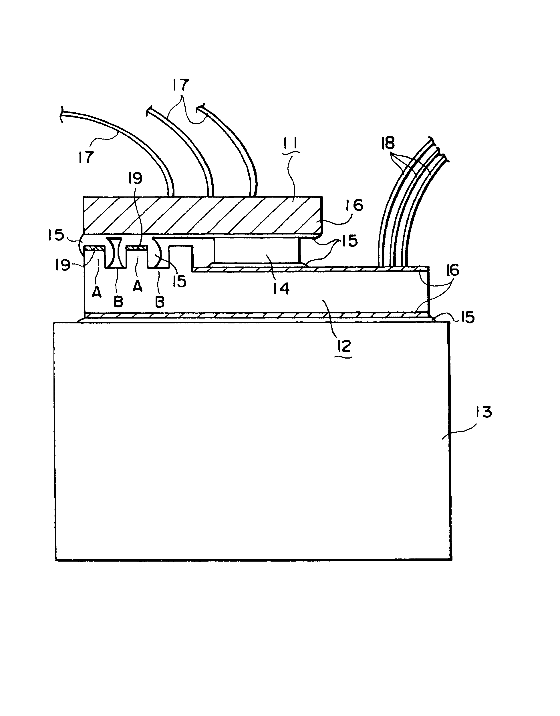
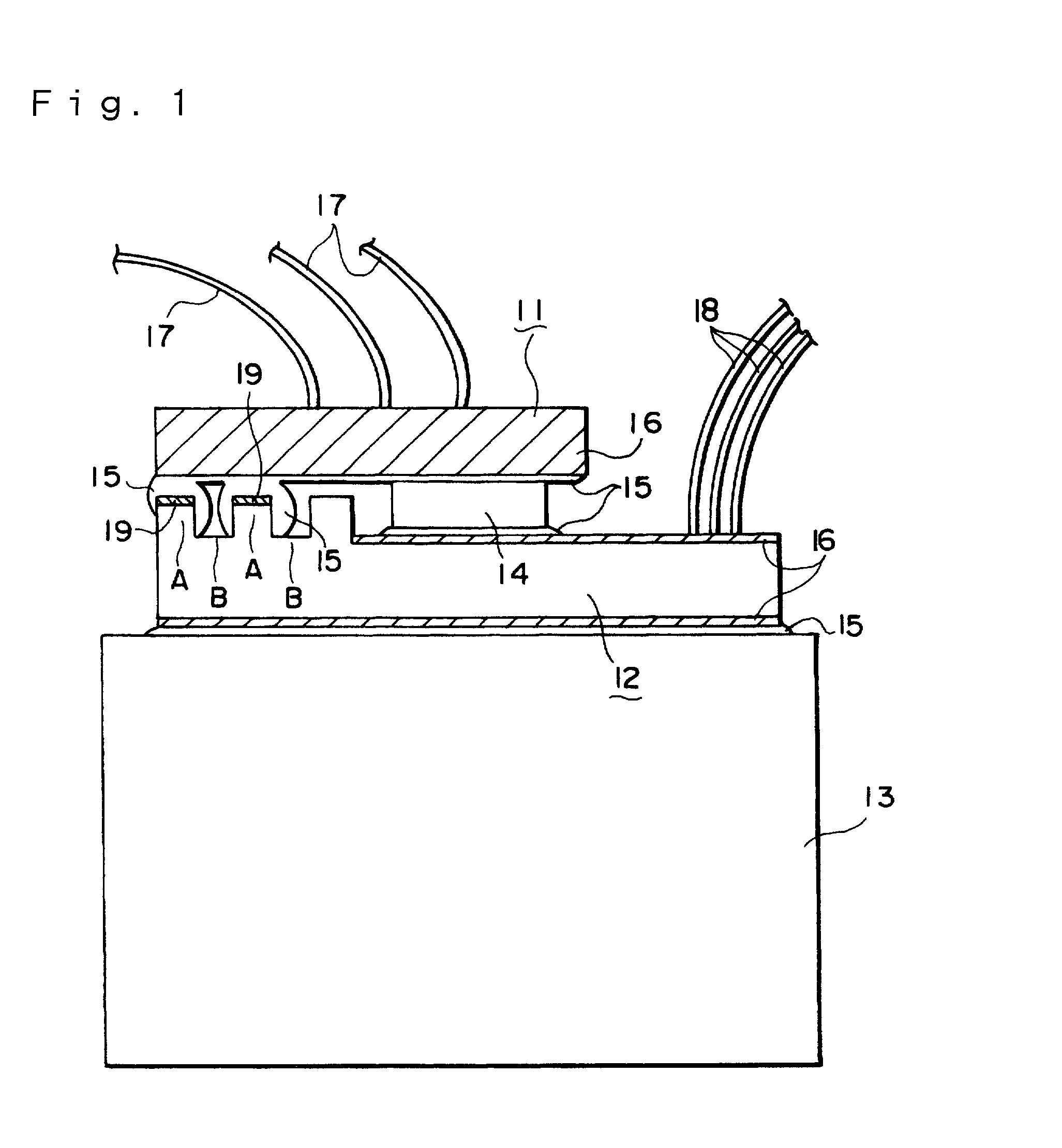
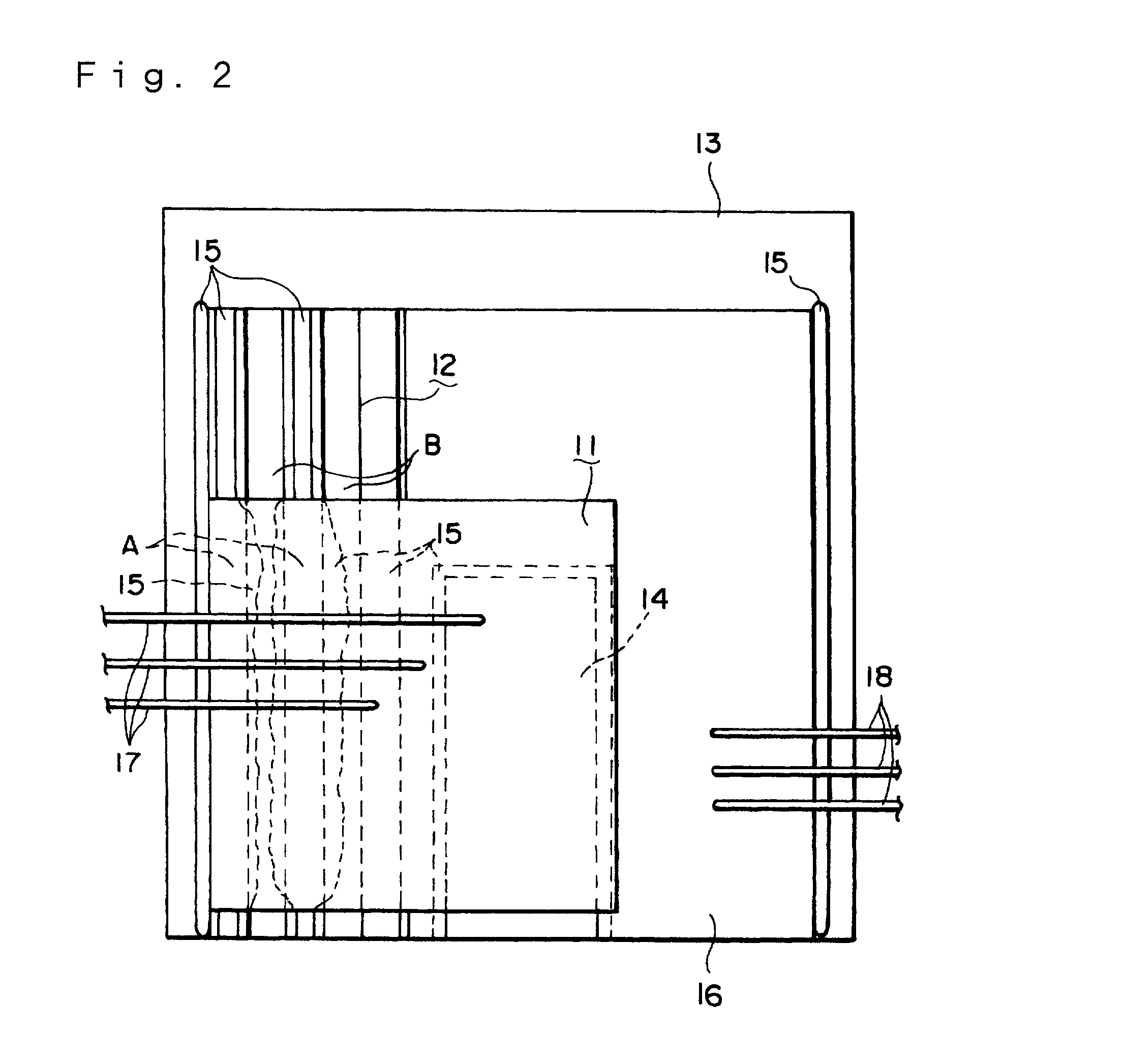
Semiconductor light emitting device
a technology of semiconductors and light emitters, applied in the direction of semiconductor lasers, semiconductor/solid-state device details, semiconductor laser structure details, etc., can solve the problems of poor reliability, remarkably declined maximum light output, and insatiable reliability of the devi
- Summary
- Abstract
- Description
- Claims
- Application Information
AI Technical Summary
Benefits of technology
Problems solved by technology
Method used
Image

Examples
example 2
[0127] The semiconductor light emitting device was fabricated similarly to Example 1 except that a CuW thin plate was used as the third heat sink 13 as shown in FIG. 3, under which a Peltier cooler was provided, an optical fiber 20 having a wedge-shaped fiber lens 21 was located so as to face the front facet of the semiconductor light emitting laser element, the device was made into a butterfly package, and that the semiconductor laser element was mounted on the second heat sink so as to be recessed towards the rear facet by approximately 10 .mu.m. The device showed, upon input of the light emitted from the fiber end, a threshold current of 18.5 mA and a slope efficiency of 0.71 mW / mA.
example 3
[0128] The semiconductor light emitting device was fabricated similarly to Example 1 except that the semiconductor light emitting element was fabricated as below, and the first heat sink was made of diamond.
[0129] The semiconductor light emitting element was fabricated similarly to Example 1 except that the cavity length was defined as 1,200 .mu.m, and that the opening of the silicon nitride mask was formed in a shape such that having a stripe pattern of 5.1 .mu.m wide, the surface extending from the front facet of the element to a position recessed by 250 .mu.m towards the rear facet, having a gradually narrowed pattern over the first 450 .mu.m, and finally having stripe pattern of 1.5 .mu.m wide over the residual 500 .mu.m range forward the rear facet.
[0130] Current-light output characteristics of such can package injected with electric current up to 2.0 A at 25.degree. C. was shown in FIG. 7. The device was found to have a threshold current of 23.1 mA, a slope efficiency of 0.84 ...
PUM
 Abstract
Description
Claims
Application Information