Embedded attenuated phase shift mask and method of making embedded attenuated phase shift mask

Inactive Publication Date: 2002-06-06
UNAXIS USA
View PDF0 Cites 34 Cited by
  • Summary
  • Abstract
  • Description
  • Claims
  • Application Information

AI Technical Summary

Benefits of technology

0015] In view of the foregoing, it would be desirable to provide an improved EAPSM structure that provides near optimal 180 degree phase shifting and a process for fabricating the EAPSM structure that does not damage the substrate layer of the EAPSM. According to one embodiment of the present invention a phase shift mask, capable of shifting a phase of

Problems solved by technology

The inventors have realized that the Halogen-based, fluorine-based RF plasma etching can also damage and/or remove a portion of the underlying quartz substrate

Method used


Image

  • Embedded attenuated phase shift mask and method of making embedded attenuated phase shift mask
  • Embedded attenuated phase shift mask and method of making embedded attenuated phase shift mask
  • Embedded attenuated phase shift mask and method of making embedded attenuated phase shift mask

Examples


Embodiment Construction

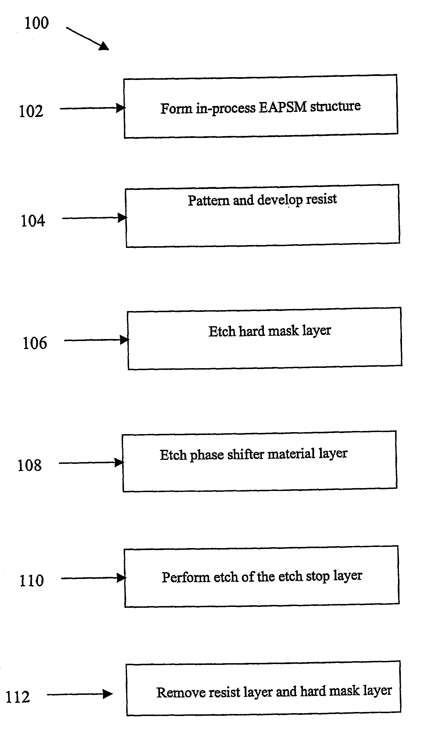
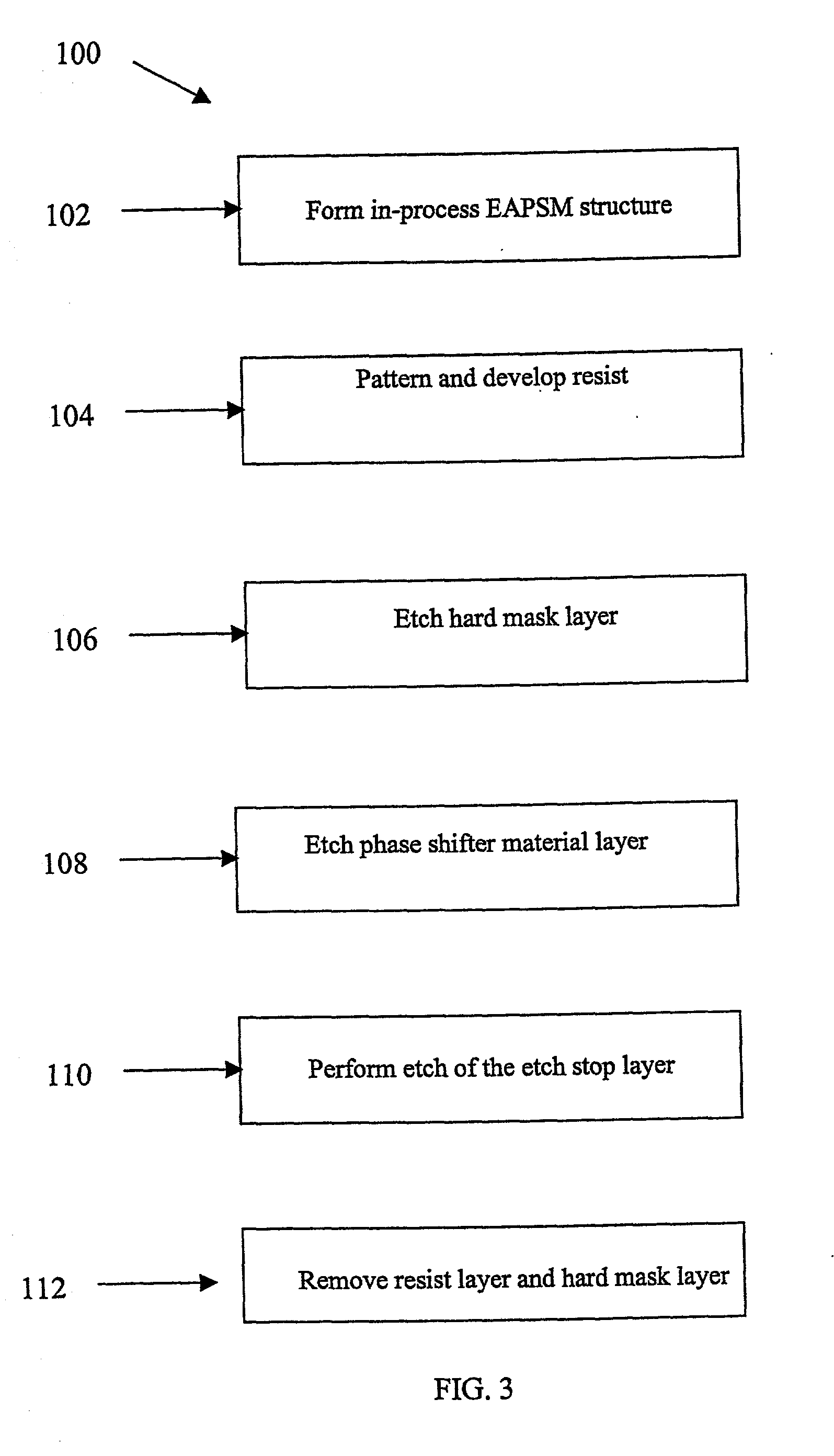
[0028] The inventors have discovered that providing an etch stop layer which has high etch selectivity with respect to a phase shifter layer can avoid damage to the substrate.

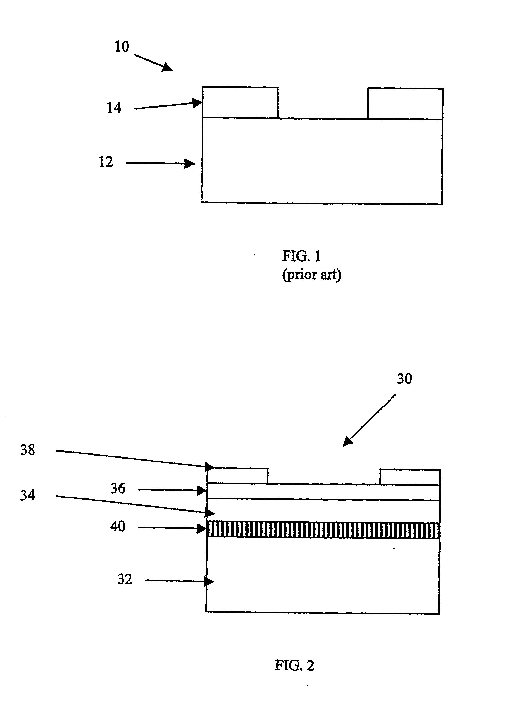
[0029] FIG. 2 illustrates one preferred embodiment of the present invention, an in-process EAPSM structure 30, which includes a transparent substrate 32, a phase shifter material layer 34, a hard mask layer 36, a resist layer 38, and an etch stop layer 40 interposed between the substrate 32 and the phase shifter layer 34.

[0030] In this embodiment, the substrate 32 comprises a material having substantial transmission properties at the operating lithographic wavelength. For example, substrate 32 can comprise any of the following materials: quartz, calcium fluoride (CaF.sub.2), or other conventional substantially transparent substrate materials. In a preferred embodiment, the substrate 32 is quartz. Substrate 32 preferably has a thickness of from about 2 millimeters (mm) to about 9 mm.

[0031] The phase shifter laye...


PUM

PropertyMeasurementUnit
Thicknessaaaaaaaaaa
Thicknessaaaaaaaaaa
Thicknessaaaaaaaaaa

Abstract

An embedded attenuated phase shift mask ("EAPSM") includes an etch stop layer that can be plasma etched in a process that is highly selective to the underlying quartz substrate. Selectivity to the underlying quartz maintains a desired 180 degree phase shift uniformly across the active mask area. Conventional plasma etching techniques can be utilized without damage to the underlying quartz substrate. Alternatively, the etch stop layer comprises a transparent material that can remain intact in the mask structure.

Description

RELATED APPLICATIONS[0001] This application claims benefit of and priority to Provisional Application Serial No. 60 / 250,351, filed on Dec. 1, 2000, entitled "EMBEDDED ATTENUATED PHASE SHIFT MASK AND METHOD OF MAKING EMBEDDED ATTENUATED PHASE SHIFT MASK," incorporated by reference in its entirety herein.BACKGROUND OF THE INVENTION[0002] 1. Field of the Invention[0003] The present invention is directed to a phase shift mask structure and a method for forming patterns on a semiconductor wafer.[0004] 2. Related Art[0005] Conventional processes for the fabrication of semiconductor wafers often incorporate a lithographic process to create a desired pattern on a semiconductor wafer. For example, optical lithography can be used to transfer an integrated circuit pattern through a mask onto a semiconductor wafer, such as a silicon wafer. Conventional masks include chromium binary masks. Openings in the mask permit light from an optical projection unit or light source, such as a laser, to irra...

Claims


Application Information

Patent Timeline
IPC IPC(8): G03F1/00
CPCG03F1/32
Inventor WESTERMAN, RUSSELLCONSTANTINE, CHRISTOPHER
Owner UNAXIS USA
Why Eureka
Try Eureka