Logical circuit

a logic circuit and circuit technology, applied in the field of logic circuits, can solve the problems of all logic gates, dcvs-domino circuits, and the area of logical gates being too large when the layout is designed, and achieve the effect of reducing the area of logic gates, and reducing the number of precharge signals

Inactive Publication Date: 2002-08-01
A I L
View PDF0 Cites 12 Cited by
  • Summary
  • Abstract
  • Description
  • Claims
  • Application Information

AI Technical Summary

Problems solved by technology

If such a gate width ratio is set, however, the area of the logical gate becomes too large when the layout thereof is designed.
The significant disadvantage of the DCVS-DOMINO is that all logical gates constituted out of the DCVS-DOMINO circuits require precharge signals.
Due to this, the precharge signal consumes much power.
Due to this, the number of NMOS transistors connected in series increases, thereby disadvantageously lowering the current driving capability of the NMOS network 90 and decelerating the operating speed thereof.
It is noted, however, that ring connection for returning the output of a basic logical gate to the input of the same logical gate through the other basic logical gate is not permitted.
According to this method, however, the gate width w of a logical gate in the next stage connected, as a load, to the output of a logical gate in the first stage is increased, with the result that load capacitance increases and sufficient acceleration effect cannot be obtained.
Besides, the problems of an increase in power consumption and an increase in the area of an LSI chip follow.
The shortening of the effective value propagation delay particularly contributes to the acceleration of the circuit operation.
Due to this, a repetition cycle for repeatedly operating the logical circuit cannot be shortened.
It is noted, however, that ring connection for returning the output of a basic logical gate to the input of the same logical gate through the other basic logical gate is not permitted.
Due to this, a repetition cycle for repeatedly operating the logical circuit cannot be shortened.

Method used


Image

  • Logical circuit
  • Logical circuit
  • Logical circuit

Examples


Embodiment Construction

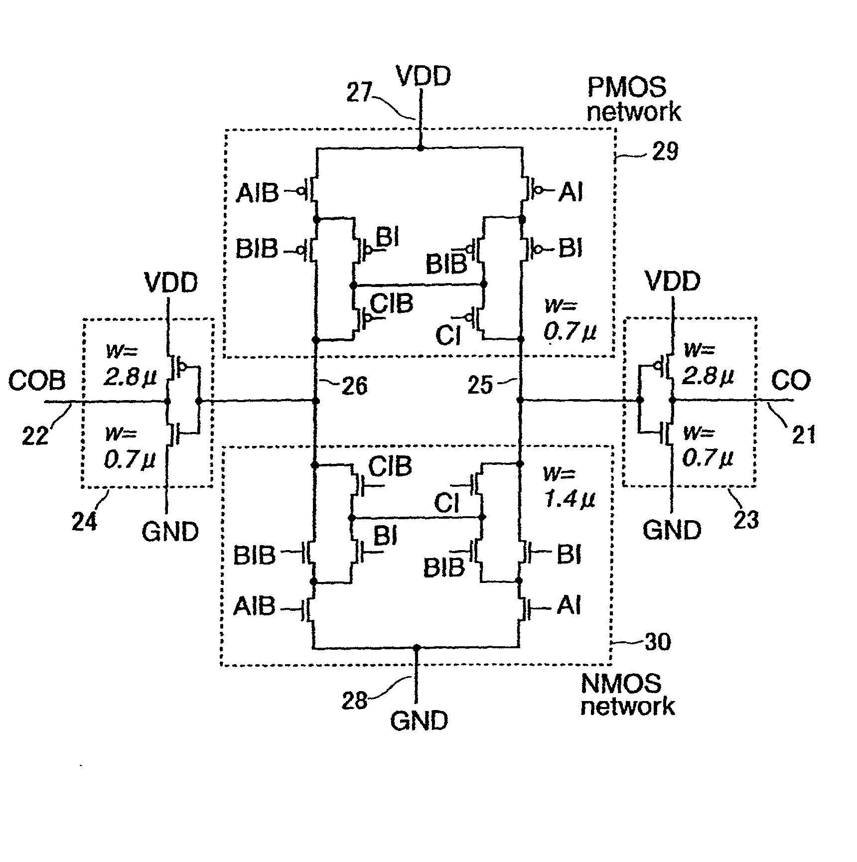
[0127] FIGS. 13 and 36 show embodiments corresponding to claims 1 to 5 and show the basic logical gates each constituted as the static circuit or the ASD-CMOS circuit. FIG. 13 shows the basic logical gate generating a carry output CO in a full adder shown in FIG. 37. FIG. 36 shows the basic logical gate generating a sum output SO in the full adder shown in FIG. 37. Both of FIGS. 13 and 36 embody the interiors of the PMOS network 29 and the NMOS network 30 in the basic logical gates shown in FIGS. 12 and 14 to 17. Common plural pairs of signal lines 20 are used as inputs in FIGS. 13 and 36 and denoted by AI and AIB, BI and BIB, CI and CIB, respectively. If all of these signal pairs have the halt values, i.e., the GND potentials, the input lines 25 and 26 of the respective output inverters 23 and 24 have the VDD potentials, respectively and one pair of signal lines 21 and 22 as the outputs has the halt value, i.e., GND potential. Next, if the signal values of all the inputs change to ...


PUM


Abstract

Very high speed operation and reduction of power consumption are realized simultaneously in a two-wire type logical circuit having a halt value and an effective value as signal values. Signal rise transition delay time and signal fall transition delay time are purposely designed asymmetrically and an effective value propagation delay is shortened, thereby accelerating an operating speed of the logical circuit. By eliminating a clock signal from a DOMINO circuit, power consumption is reduced. An architecture for concealing a halt value propagation delay is employed.

Description

[0001] 1. Field of the Invention[0002] The present invention relates to a logical circuit used for constituting an LSI, and particularly belongs to a circuit design technique for improving the operating speed of the logical circuit and for reducing power consumption, so as to accelerate a two-wire logical circuit using two signal lines to express a logical value.[0003] 2. Description of the Related Art[0004] A logical gate is used as a constituent element for a digital LSI manufactured by CMOS process. As shown in FIG. 1, a standard CMOS logical gate is constituted such that a PMOS network 97 consisting of PMOS transistors are arranged between a VDD power source line 27 and an output 96 and that an NMOS network 98 comprising NMOS transistors 98 are arranged between a GND power source line 28 and the output 96. Either the PMOS network 97 or the NMOS network 98 becomes conductive in accordance with the value of an input 95 and outputs either a VDD potential or a GND potential to the o...

Claims


Application Information

Patent Timeline
Patent Type & Authority Applications(United States)
IPC IPC(8): G06F7/50G06F7/501H03K19/0948H03K19/096
CPCG06F7/5016H03K19/0948H03K19/0963
Inventor TAKI, KAZUO
Owner A I L
Why Eureka
Try Eureka