Photomask blank and photomask

a technology of photomask and blank, which is applied in the field of photomask blank and photomask, can solve the problems of ineffective surface roughness of seed layer less than 0.5 nm thick, low productivity, and long time consumption

Inactive Publication Date: 2002-08-22
SHIN ETSU CHEM IND CO LTD
View PDF0 Cites 29 Cited by
  • Summary
  • Abstract
  • Description
  • Claims
  • Application Information

AI Technical Summary

Benefits of technology

[0012] The invention is directed to a photomask blank or photomask comprising a transparent substrate, at least one layer of light-shielding film and at least one layer of antireflective film both on the substrate. It has been found that when a seed layer is formed between the transparent substrate and the light-shielding film or the antireflective film, the light-shielding film or the antireflective film is improved in surface flatness whereby a photomask blank or photomask having uniformity of film quality is obtained.
[0015] According to the invention, the seed layer on the transparent substrate presents growth nuclei for the light-shielding film or the antireflective film so that the film grows on the seed layer while creating fine grains. Then the interposition of the seed layer eventually endows the photomask blank or photomask with a reduced surface roughness.

Problems solved by technology

A seed layer of less than 0.5 nm thick may be ineffective for improving surface roughness.
A seed layer of more than 10 nm thick may achieve no additional improvement and take a longer time to deposit, resulting in low productivity.

Method used


Image

  • Photomask blank and photomask
  • Photomask blank and photomask
  • Photomask blank and photomask

Examples


example 1

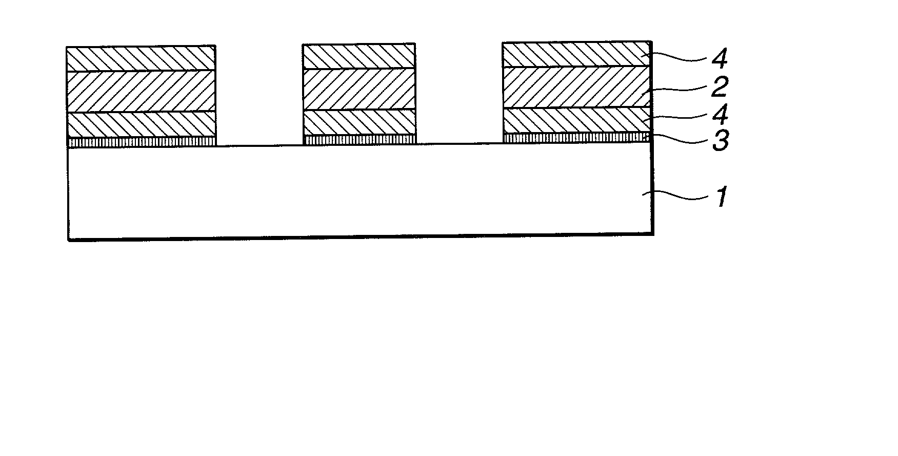
[0043] On a 6-inch quartz substrate, a CrCON film of 3 nm thick was deposited as the seed layer by DC sputtering. Metallic chromium was used as the target, and the gases passed through the system were Ar (32 sccm) as the sputtering gas and CO.sub.2 (1.0 sccm) and N.sub.2 (18 sccm) as the reactive sputtering gas. Other sputtering conditions included a gas pressure during discharge of 0.3 Pa and a power of 7.1 W / cm.sup.2. The composition of the CrCON film was 48 atom % chromium, 9 atom % carbon, 17 atom % oxygen and 26 atom % nitrogen, as determined by electron spectroscopy for chemical analysis (ESCA).

[0044] Next, another CrCON film was deposited to a thickness of 70 nm on the seed layer (CrCON film) by DC sputtering. Chromium was used as the target, and the gases passed through the system were Ar (32 sccm), CO.sub.2 (0.7 sccm) and N.sub.2 (1 sccm). Other sputtering conditions included a gas pressure during discharge of 0.3 Pa and a power of 6.6 W / cm.sup.2. The composition of the CrC...

example 2

[0047] On a 6-inch quartz substrate, a CrCON film of 3 nm thick was deposited as the seed layer by DC sputtering. Metallic chromium was used as the target, and the gases passed through the system were Ar (32 scam) as the sputtering gas and CO.sub.2 (1.0 scam) and N.sub.2 (18 scam) as the reactive sputtering gas. Other sputtering conditions included a gas pressure during discharge of 0.3 Pa and a power of 7.1 W / am.sup.2. The composition of the CrCON film was 48 atom % chromium, 9 atom % carbon, 17 atom % oxygen and 26 atom % nitrogen, as determined by ESCA.

[0048] Next, another CrCON film was deposited to a thickness of 25 nm on the seed layer (CrCON film) by DC sputtering. Chromium was used as the target, and the gases passed through the system were Ar (32 sccm), CO.sub.2 (14 sccm) and N.sub.2 (10 scam). Other sputtering conditions included a gas pressure during discharge of 0.3 Pa and a power of 6.6 W / Cm.sup.2. The composition of the CrCON film was 42 atom % chromium, 5 atom % carbo...


PUM

PropertyMeasurementUnit
thicknessaaaaaaaaaa
surface roughnessaaaaaaaaaa
thicknessaaaaaaaaaa

Abstract

In the manufacture of a photomask blank, a seed layer of a chromium material containing oxygen, nitrogen and / or carbon is formed on a transparent substrate before a light-shielding film and an antireflective film are deposited thereon. Any film on the seed layer builds up in accordance with fine granular growth, and so the resulting photomask blank has an improved surface roughness, which enables high-sensitivity detection in the process of defect inspection and circuit pattern inspection. By lithographically patterning the photomask blank, a photomask is fabricated.

Description

[0001] 1. Field of the Invention[0002] The present invention relates to a photomask blank and a photomask for use in the fabrication of semiconductor integrated circuits and high-density integrated circuits.[0003] 2. Prior Art[0004] Photolithographic processes involving the use of photomasks are employed in the fabrication of high-density semiconductor integrated circuits such as LSI and VLSI chips, color filters for charge-coupled devices and liquid-crystal displays, and magnetic heads.[0005] Photomasks used for microfabrication are produced from a photomask blank composed of a transparent substrate such as quartz glass or aluminosilicate glass and a light-shielding film, typically in the form of a chromium film, deposited thereon by a sputtering or vacuum evaporation technique. The photomask is created by forming a specific pattern in the light-shielding film of the photomask blank.[0006] The chromium-based light-shielding film has a high light reflectance. To prevent light which ...

Claims


Application Information

Patent Timeline
Patent Type & Authority Applications(United States)
IPC IPC(8): G03F1/50G03F1/54G03F7/20H01L21/027
CPCG03F1/14G03F1/50G03F1/68G03F1/38G03F1/46
Inventor TSUKAMOTO, TETSUSHIKANEKO, HIDEOMARUYAMA, TAMOTSUINAZUKI, YUKIOSHINAGAWA, TSUTOMUOKAZAKI, SATOSHI
Owner SHIN ETSU CHEM IND CO LTD
Why Eureka
Try Eureka