
Memory module and computer system comprising a memory module

a memory module and computer system technology, applied in the field of memory modules, can solve the problems of high cost of motherboards and other devices which support and interface with rimms, stringent interface and clocking signal requirements, and reduce the external effect of clocks, reduce signal reflection, and reduce clock pinout

Inactive Publication Date: 2002-09-05
INTEL CORP
View PDF0 Cites 17 Cited by
  • Summary
  • Abstract
  • Description
  • Claims
  • Application Information

AI Technical Summary

Benefits of technology

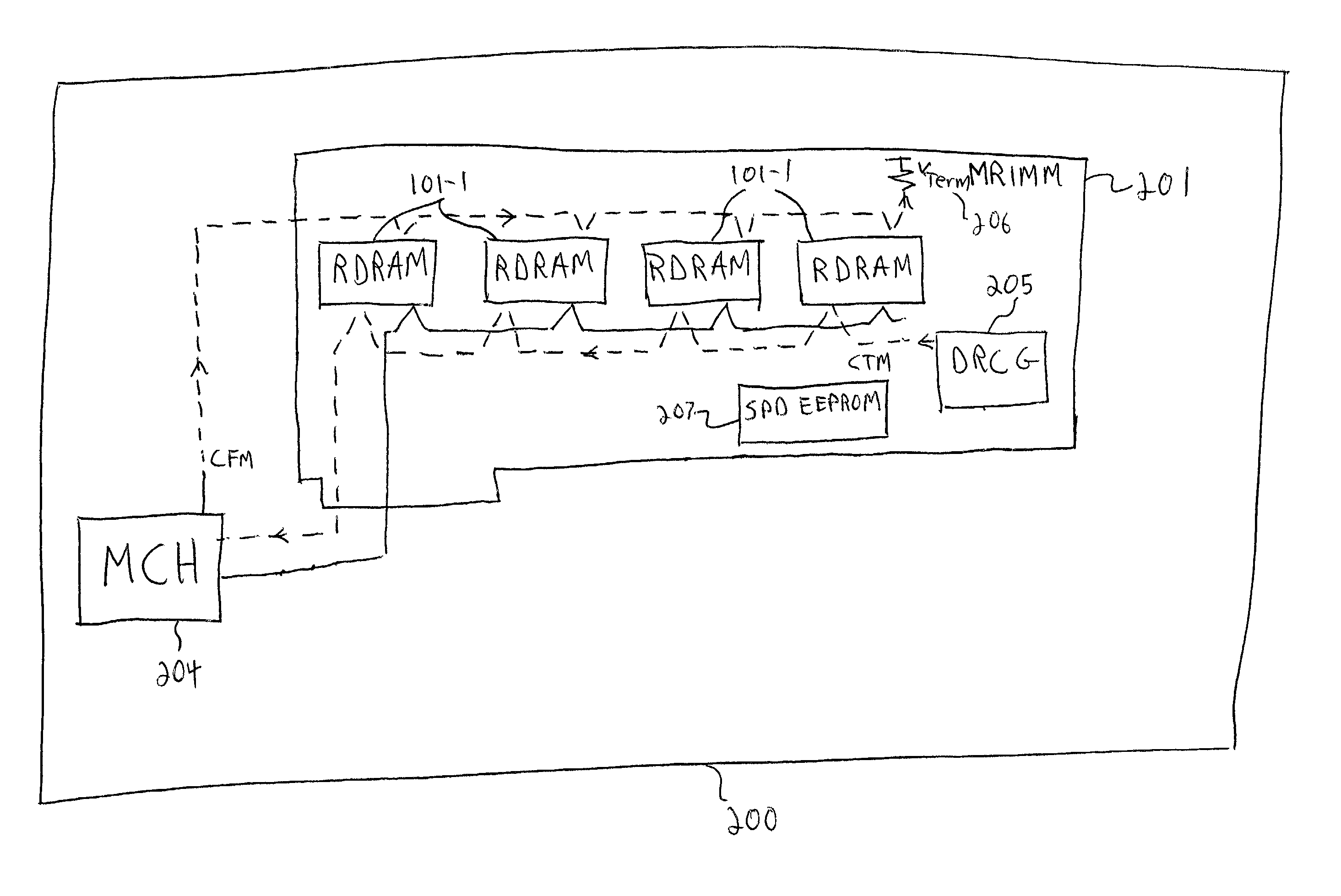
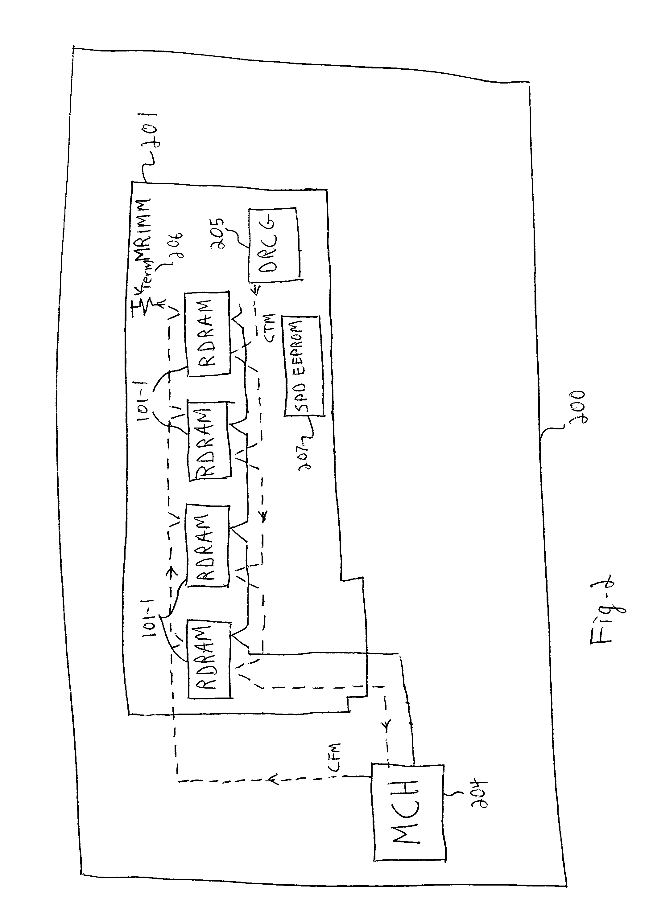
[0019] FIG. 3 is a schematic diagram illustrating the external connections of MRIMM 201 shown in FIG. 2. As explained, clock pins are not needed for clock signals to enter and exit the module. This allows the clock pinout to be reduced to approximately half that of the conventional RIMM module, and reduces signal reflections at the connector, and thereby reduces external effects on the clocks. The Rambus memory module 201 has only the 92 total pins listed in Table 1 below, yet still supports a plurality of 16-bit RDRAM devices. (The RDRAM devices may operate at 800 MHz or 600 MHz, and may have a capacity of 64 Mb, 128 Mb or 256 Mb.) FIGS. 6A and 6B are schematic diagrams illustrating the connections of the memory devices of RIMM 201 in the example embodiment of the invention shown in FIG. 2.1 TABLE 1 Pin Pin Name Pin Pin Name A1 Gnd B1 Gnd A2 NC B2 LDQA7 A3 Gnd B3 Gnd A4 LDQA6 B4 LDQA5 A5 Gnd B5 Gnd A6 LDQA4 B6 LDQA3 A7 Gnd B7 Gnd A8 LDQA2 B8 LDQA1 A9 Gnd B9 Gnd A10 LDQA0 B10 LCFM A11 Gnd B11 Gnd A12 LCTMN B12 LCFMN A13 Gnd B13 Gnd A14 LCTM B14 NC A15 Gnd B15 Gnd A16 NC B16 LROW2 A17 Gnd B17 Gnd A18 LROW1 B18 LROW0 A19 Gnd B19 Gnd A20 LCOL4 B20 LCOL3 A21 Gnd B21 Gnd A22 LCOL2 B22 LCOL1 A23 Gnd B23 Gnd A24 LCOL0 B24 LDQB0 A25 Gnd B25 Gnd A26 LDQB1 B26 LDQB2 A27 Gnd B27 Gnd A28 LDQB3 B28 LDQB4 A29 Gnd B29 Gnd A30 LDQB5 B30 LDQB6 A31 Gnd B31 Gnd A32 LDQB7 B32 PWRDNB A33 Gnd B33 Gnd A34 LSCK B34 LCMD A35 VTERM(1.8) B35 VTERM(1.8) A36 SA2 B36 SIN A37 VTERM(1.8) B37 VTERM(1.8) A38 Gnd B38 Gnd A39 Gnd B39 Gnd A40 CLKN B40 CLKM A41 VDD(3.3) B41 VDD(3.3) A42 VDD(3.3) B42 VDD(3.3) A43 DRCG1.8 B43 DRCG3.3 A44 REFCLK B44 SWP A45 SPD3.3 B45 S0 / S1 A46 SMBCLK B46 SMBDAT
[0020] In addition to reducing the pin count for a smaller memory module, placing DRCG 205 and its associated components (decoupling, misc. discrete components) on RIMM 201 alleviates the problem of motherboard space constraints. The example embodiment also addresses the problem of RIMM form factor in the use of a graphics memory implementation. It is a smaller memory module for small form factor motherboards referred to hereafter as a Miniature RIMM ("MRIMM"). It is 35.0 mm in height with an approximate weight of 30 grams (about 2 / 3 that of a standard RIMM module).

Problems solved by technology

However, a RIMM has stringent interface and clocking signal requirements.
Such requirements generally make the motherboards and other devices which support and interface with RIMMs more expensive than devices which support and interface with other types of memory modules.

Method used


Image

  • Memory module and computer system comprising a memory module
  • Memory module and computer system comprising a memory module
  • Memory module and computer system comprising a memory module

Examples


Embodiment Construction

[0022] Maximum warpage of the PC board comprising MRIMM 201 is 1% (0.01 mm per mm). Impedance for the loaded and unloaded sections of all critical signal traces on MRIMM 201 are at 28 ohms + / -10%. The critical signals include the RSL signals, two high-speed CMOS signals (LSCK and LCMD) and the clock signals.

[0023] DRCG 205 may supply a 300 or 400 MHz differential clock signal pair to support the Direct Rambus memory subsystem composed of RDRAM memory devices 101-1. It includes signals to synchronize the Direct Rambus Channel clock to an external system clock. Control and data signals are clocked on both edges of the clock resulting in an 600 or 800 MHz effective transfer. Power consumption for DRCG 205 is less than 350 mW with Vdd=3.3V.+-.5%. FIG. 4 is a schematic diagram illustrating the connections of Direct Rambus Clock Generator (DRCG) 205 in the example embodiment of the invention shown in FIG. 2.

[0024] Although not shown in FIG. 2, MCH 204 is preferably an integrated circuit c...


PUM


Abstract

A memory module comprises at least one memory device, a clock generator providing clocking signals, and a clocking topology providing the clocking signals to said at least one memory device.

Description

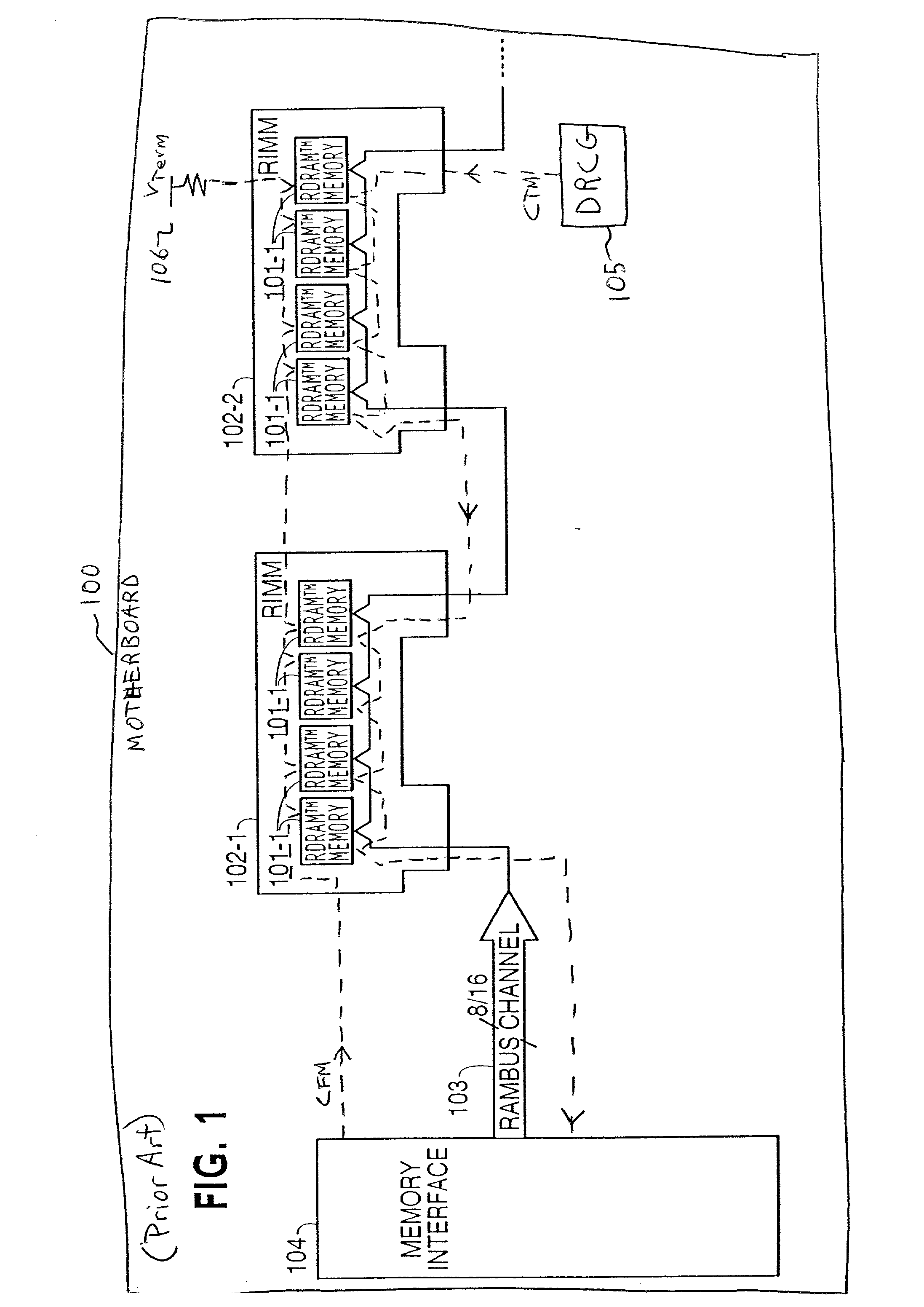
[0001] 1. Field of the Invention[0002] This invention relates generally to memory modules. In particular, the present invention relates to a memory module having its own clock generator.[0003] 2. Description of the Related Art[0004] Some processing systems or functions in processing systems may have stringent memory processing requirements and thus utilize a type of memory module which is well suited to those processing requirements. One type of memory module specifically designed to have higher operating characteristics is a Rambus In line Memory Module ("RIMM"), available for license from Rambus, Inc. of Mountain View, Calif. However, a RIMM has stringent interface and clocking signal requirements. Such requirements generally make the motherboards and other devices which support and interface with RIMMs more expensive than devices which support and interface with other types of memory modules.[0005] FIG. 1 illustrates a conventional installation of a plurality of RIMM.TM. memory m...

Claims


Application Information

Patent Timeline
IPC IPC(8): G11C5/00
CPCG11C5/04G11C5/06
Inventor JOLIN, EDWARD M.DELINO, JULIUS
Owner INTEL CORP
Learn More