Organic electroluminescent device

a technology of electroluminescent devices and electroluminescent tubes, which is applied in the direction of discharge tube luminescnet screens, natural mineral layered products, etc., can solve the problems of difficult color emission, low luminance, and high cost of peripheral driving circuits, and achieve light emission efficiency, inhibit the deterioration of luminance, and high efficiency

Inactive Publication Date: 2002-09-12
MITSUBISHI CHEM CORP
View PDF1 Cites 123 Cited by
  • Summary
  • Abstract
  • Description
  • Claims
  • Application Information

AI Technical Summary

Benefits of technology

0035] More specifically, the present inventors have found that when the constituent element (2), namely, Compound A capable of phosphorescence emission at room temperature is used in combination with the constituent element (3), namely, Compound B which is (a) a phosphorescent compound of not emitting light with high efficiency by itself or (b) a fluorescent compound of emitting light in various colors but incapable of ensuring light emission efficiency as high as that of the phosphorescent compound for any of those colors, Compound A plays a role of sensitizer and the light emission of Compound B is intensified.
0036] As a result, a device capable of emitting light in various colors can be obtained and accordingly, this is very useful in realizing a flat panel display of multi-color display

Problems solved by technology

However, the EL device fabricated from the above-described inorganic material has problems such that:
3) full color emission is difficult (particularly blue) and
4) the peripheral driving circuit costs highly.
However, only an extremely low luminance could be obtained.
Thereafter, use of an europium complex is studied with an attempt to utilize the triplet excitation state, however, high light emission efficiency could not be attained either by this use.
The organic electroluminescent device using the phosphorescence molecule (T-2) described in the above-described publication emits light with relatively high efficiency, however, the organic electroluminescent device using (T-1) is low in the light emission efficiency as compared with devices using (T-2).
However, use of a phosphorescent substance alone suffers from bad stability of film and low mobility of electric charge (hole or electron) injected from electrodes and accordingly, the light emission efficiency is not elevated.
On the other hand, use of a host material alone cannot provide light emission from a triplet exciton and the material uses its energy mostly for heat and is deactivated, as a result, the light emission efficiency is not elevated.
However, this method involves energy transfer and unless the excited triplet level in the host material is close to the excited triplet level of the phosphorescent substance, the probability of energy transfer decreases and the triplet excitons cannot contribute to the light emission.
However

Method used


Image

  • Organic electroluminescent device
  • Organic electroluminescent device
  • Organic electroluminescent device

Examples


Embodiment Construction

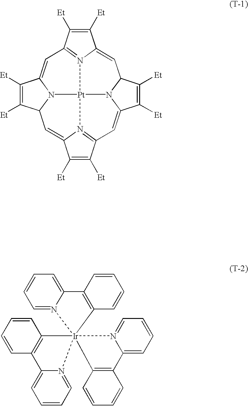
[0047] The present invention relates to an organic electroluminescent device containing a host material, Compound A capable of phosphorescence emission at room temperature and Compound B capable of phosphorescence emission or fluorescence emission at room temperature in the light-emitting layer, and having a maximum light emission wavelength attributable to Compound B. In the organic electroluminescent device, the light-emitting layer preferably contains the host material as a main component and Compound A and Compound B as sub-components.

[0048] The term "main component" as used herein means a material occupying 50% by weight or more in the materials constituting the layer and the term "sub-component" means a material occupying less than 50% by weight in the materials constituting the layer. That is, the term "contains Compounds A and B as sub-components" means that the total amount of Compound A and Compound B is less than 50% by weight based on the materials for forming the light-...


PUM

PropertyMeasurementUnit
Lengthaaaaaaaaaa
Molecular weightaaaaaaaaaa
Fluorescenceaaaaaaaaaa

Abstract

An organic electroluminescent device is disclosed, comprising a substrate having thereon a light-emitting layer sandwiched by an anode and a cathode, wherein the light-emitting layer comprises at least: (1) a host material having electron-transporting or hole-transporting property, (2) Compound A capable of phosphorescence emission at room temperature, and (3) Compound B capable of phosphorescence emission or fluorescence emission at room temperature and having the maximum light emission wavelength longer than the maximum light emission wavelength of Compound A, and the maximum light emission wavelength of said device is attributable to said (3). The light emission attributable to (3) is intensified by (2) to elevate the light emission efficiency and by selecting a fluorescent compound as (3), the device can be prevented from aging deterioration of the luminance.

Description

FIELD OF THE INVENTION[0001] The present invention relates to an organic electroluminescent device. More specifically, the present invention relates to a thin film-type device which emits light upon application of an electric field to a light-emitting layer comprising an organic compound.BACKGROUND OF THE INVENTION[0002] In conventional thin film-type electroluminescent (EL) devices, an inorganic material group II-VI compound semiconductor such as ZnS, CaS and SrS is generally doped with Mn or a rare earth element (e.g., Eu, Ce, Tb, Sm) as a emission center. However, the EL device fabricated from the above-described inorganic material has problems such that:[0003] 1) a.c. (alternating current) driving is necessary (from 50 to 1,000 Hz),[0004] 2) the driving voltage is high (up to 200 V),[0005] 3) full color emission is difficult (particularly blue) and[0006] 4) the peripheral driving circuit costs highly.[0007] In recent years, however, for the purpose of improving the above-describ...

Claims


Application Information

Patent Timeline
IPC IPC(8): H01L51/00H01L51/30H01L51/50
CPCH01L51/0052H01L51/0059H01L51/006H01L51/0065H01L51/0068H01L51/0071H01L51/0072H01L51/0077H01L51/0081H01L51/0084H01L51/0085H01L51/009H01L51/5016Y10S428/917H10K85/615H10K85/631H10K85/653H10K85/633H10K85/655H10K85/657H10K85/6572H10K85/30H10K85/341H10K85/361H10K85/324H10K85/342H10K50/11H10K2101/10
Inventor SATO, HIDEKISATO, YOSHIHARUFUGONO, MASAYO
Owner MITSUBISHI CHEM CORP
Why Eureka
Try Eureka