Optical multilayer structure material and process for producing the same, light switching device, and image display apparatus

a multi-layer structure and optical technology, applied in the field of optical multi-layer structure materials and processes for producing the same, light switching devices, image display apparatus, can solve the problems of complicated structure of display, small operation speed of liquid crystal and dmd, and complex structure of display, etc., to achieve stable and fast response, improve the strength of the supporting portion, and achieve the effect of easy reach

Inactive Publication Date: 2002-09-12
SONY CORP
View PDF3 Cites 67 Cited by
  • Summary
  • Abstract
  • Description
  • Claims
  • Application Information

AI Technical Summary

Benefits of technology

0028] As mentioned above, in each of the optical multilayer structure material, the process for producing an optical multilayer structure material, and the light switching device of the present invention, the circumference of the movable portion in the optical thin film is uniformly supported by the supporting portion. Therefore, not only can an occurrence of a phenomenon in which the optical thin film suffers strain in a specific direction be prevented, but also an effect is obtained such that a stable fast response can be achieved.
0029] Especially in the optical multilayer structure material wherein the supporting portion in the optical thin film slopes at an oblique angle to the surface of the substrate as a ground and the conductive layer, the strength of the supporting portion is improved.
0030] In addition, especially in each of the optical multilayer structure material and the process for producing an optical multilayer structure material wherein the optical thin film has, in at least one of the movable ...

Problems solved by technology

Displays, such as a projector, can be realized using the above devices, but the liquid crystal and the DMD have a small operation speed.
Therefore, for realizing a display as a light valve using the liquid crystal or DMD, the liquid crystals or DMDs must be two-dimensionally arranged, causing the structure of the display to be complicated.
However, the GLV ...

Method used


Image

  • Optical multilayer structure material and process for producing the same, light switching device, and image display apparatus
  • Optical multilayer structure material and process for producing the same, light switching device, and image display apparatus
  • Optical multilayer structure material and process for producing the same, light switching device, and image display apparatus

Examples


first embodiment

[0053] [First Embodiment]

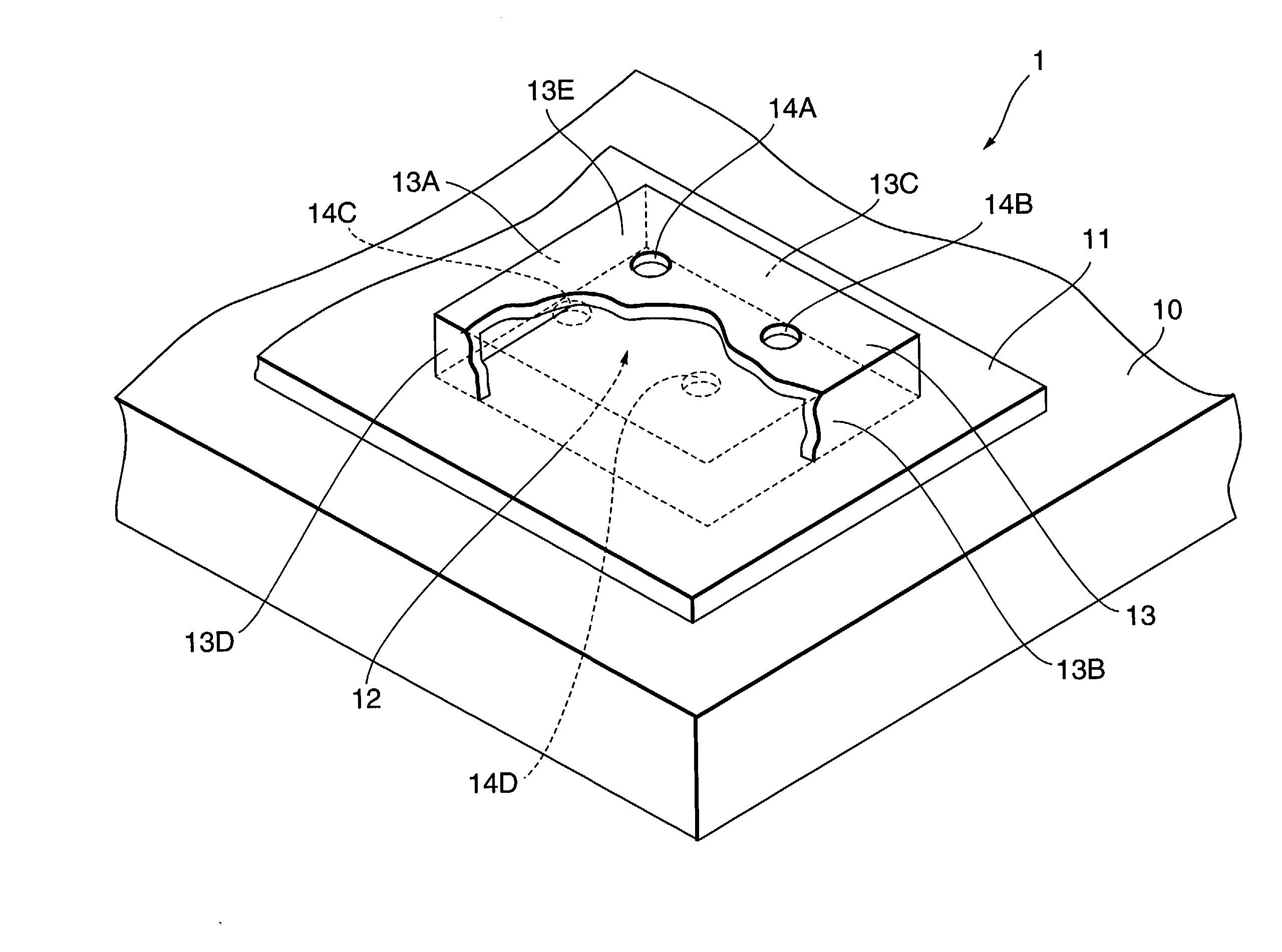
[0054] FIG. 3 shows the basic construction of an optical multilayer structure material 1 according to the first embodiment of the present invention. The optical multilayer structure material 1 is specifically used as, for example, a light switching device, and a plurality of the light switching devices are arranged in a one-dimensional array form to constitute an image display apparatus.

[0055] The optical multilayer structure material 1 of the present embodiment has a construction such that, on a substrate 10 comprised of a nonmetallic transparent material, such as transparent glass or a transparent plastic, a conductive layer 11 in contact with the substrate 10, a gap portion 12 having a size that enables an interference phenomenon to occur and can be changed, and an optical thin film 13 having a movable portion are formed in this order.

[0056] The conductive layer 11 may be a composite layer comprised of a plurality of layers, and has a function as a lower ...

second embodiment

[0070] [Second Embodiment]

[0071] In the present embodiment, as shown in FIG. 9, a movable portion 43B in an optical thin film 43 has a plane in a circular form, and the sidewall of its circumference serves as a supporting portion 43A. The plane form of the movable portion 43B is not limited to the circular form but may be other forms containing a curve, such as an elliptic form and a form such that the two sides in a rectangle are curved. In the movable portion 43B in the optical thin film 43, through holes 44A, 44B, 44C, 44D for allowing the etchant to reach the sacrifice layer are formed in the step of etching for sacrifice layer.

[0072] In the present embodiment, the optical thin film 43 has a plane in a circular form. Therefore, the stress is not locally concentrated on a specific portion of the movable portion 43B, and, like in the first embodiment, an optical multilayer structure material having a simple construction which can suppress generation of strain due to an internal st...

third embodiment

[0074] [Third Embodiment]

[0075] In the present embodiment, as shown in FIG. 10, unlike in the first embodiment, supporting portions 53A, 53B, 53C, 53D of the four sides of an optical thin film 53 in a rectangular form are not perpendicular to the conductive layer 11 but slope at an oblique angle of, for example, about 30.degree., and they have substantially the same thickness as that of a movable portion 53E. As mentioned above, the optical thin film 53 is deposited by the above-mentioned CVD process or vacuum deposition process and, in the deposition, the probability of particles to be deposited entering the substrate vertically is high, and, when each of the supporting portions 53A to 53D is intended to vertically stand, the amount of the particles deposited to be supporting portions is small, so that the resultant supporting portions have a small thickness, as compared to that of the movable portion 53E, thus causing the strength of the supporting portions to be lowered. By contr...


PUM


Abstract

An optical multilayer structure material has a structure such that, on a substrate, a conductive layer in contact with the substrate, a gap portion having a size that enables an interference phenomenon to occur and can be changed, and an optical thin film are formed in this order. The circumference of a movable portion in the optical thin film is uniformly supported by supporting portions, suppressing generation of strain due to an internal stress. Through holes are formed in the movable portion to allow an etchant to easily reach a sacrifice layer when forming a gap portion by etching for sacrifice layer. There is provided an optical multilayer structure material having a simple construction, which can suppress generation of strain due to an internal stress and can be advantageously used in an image display apparatus.

Description

CROSS REFERENCES TO RELATED APPLICATIONS[0001] The present document is based on Japanese Priority Document JP 2001-003001, filed in the Japanese Patent Office on Jan. 10, 2001, the entire contents of which being incorporated herein by reference.BACKGROUND OF THE INVENTION[0002] 1. Field of the Invention[0003] The present invention relates to an optical multilayer structure material having a function of reflecting or transmitting a light and a process for producing the same, and a light switching device and an image display apparatus each using the optical multilayer structure material.[0004] 2. Description of the Related Art[0005] In recent years, displays are very important as a display device for image information, and, as a device for the displays, especially as a device for optical communication, optical recording apparatuses, and optical printers, a development of a light switching device (light valve) which operates at a high speed is desired. As conventional devices of this t...

Claims


Application Information

Patent Timeline
IPC IPC(8): G02B26/08B81B3/00G02B5/28G02B26/00G02B26/02
CPCG02B26/001G02B26/02
Inventor ISHIKAWA, HIROICHIMAKINO, TAKUYAWATANABE, HIDENORIHONJO, YOSHIHARU
Owner SONY CORP
Why Eureka
Try Eureka