Semiconductor device and method of manufacturing the same

a technology of semiconductor devices and semiconductors, applied in semiconductor devices, semiconductor/solid-state device details, electrical apparatus, etc., can solve the problems of high recovery voltage, increase in reverse recovery loss, and electric loss

Inactive Publication Date: 2002-09-19
FUJI ELECTRIC CO LTD
View PDF2 Cites 58 Cited by
  • Summary
  • Abstract
  • Description
  • Claims
  • Application Information

AI Technical Summary

Benefits of technology

0026] According to a third aspect of the invention, there is provides a semiconductor device including: a bulk wafer including a first drift layer of a first conductivity type, the bulk wafer having a first major surface and a second major surface; a buffer layer of the first conductivity type on the first major surface of the bulk wafer, the buffer layer being doped more heavily than the first drift layer by implanting an impurity of the first conductivity type; a second drift layer of the first conductivity type epitaxially grown on the buffer layer, the second drift layer being doped more lightly than the buffer layer; an anode layer formed by implanting an impurity of a second conductivity type into the second drift layer; an anode electrode on the anode layer; a cathode layer on the surface of the bulk wafer exposed by grinding back the bulk wafer for a predetermined depth from the second major surface thereof, the cathode layer being doped more heavily than the first drift layer by implanting an impurity of the first conductivity type; and a cathode electrode on the cathode layer.
0027] According to a fourth aspect o

Problems solved by technology

The electrical loss, that is the product of the high reverse recovery current and the reverse recovery voltage, is high.
However, when too many carriers are accumulated in the drift layer in the ON-state of the diode, the reverse recovery loss increases and it takes a long time until the reverse recovery ends; that is the reverse recovery time is elongated.
However, lowering of the breakdown voltage and increase of the leakage current under the applied reverse bias voltage are caused more often in the low-injection-type diodes than in the pin diode having the drift layer of the same thickness due to the Schottky junction or the lightly doped anode layer.
Local lifetime control conducted by irradiatin

Method used


Image

  • Semiconductor device and method of manufacturing the same
  • Semiconductor device and method of manufacturing the same
  • Semiconductor device and method of manufacturing the same

Examples


Embodiment Construction

[0066] Now the invention will be explained in detail hereinafter with reference to the accompanied drawing figures which illustrate the preferred embodiments of the invention. In the following descriptions, the first conductivity type is an n-type and the second conductivity type is a p-type.

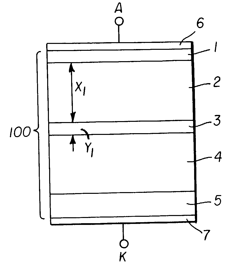
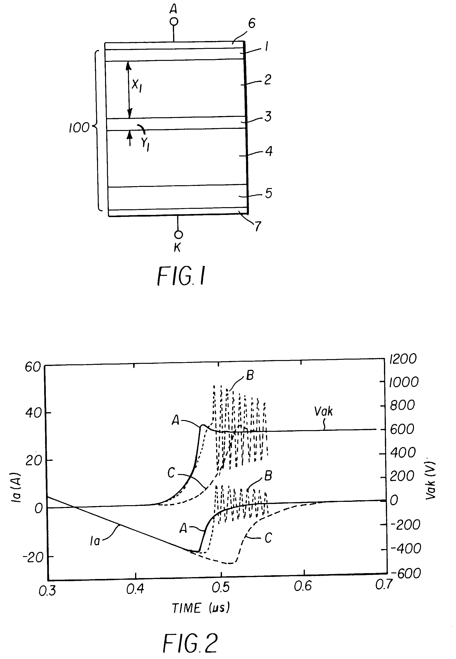
[0067] FIG. 1 is a cross sectional view of a semiconductor device according to a first embodiment of the invention. FIG. 1 shows the active region of a pin diode, which includes an n-type buffer layer. The breakdown withstanding region of the pin diode is omitted from the figure. The pin diode according to the first embodiment is formed in the following way. A second n-type drift layer 4 is epitaxially grown on an n-type semiconductor substrate doped, for example, with Sb (antimony) and exhibiting low specific resistance of 0.01 .OMEGA.-cm. The n-type semiconductor substrate will be an n-type cathode layer 5. Second n-type drift layer 4 is 55 .mu.m in thickness, doped, for example, with P (phosp...


PUM


Abstract

A semiconductor device, such as a pin diode, includes a first drift layer, a second drift layer, an anode layer on the first drift layer, and a buffer layer formed between the first and second drift layers. The shortest distance from the pn-junction between the anode layer and the buffer layer, and the thickness of the buffer layer are set at the respective values at which a high breakdown voltage is obtained, while reducing the tradeoff relation between the soft recovery and the fast and low-loss reverse recovery.

Description

BACKGROUND[0001] The present invention relates to semiconductor devices such as diodes. FIG. 25 is a cross sectional view of a conventional pin diode. Referring now to FIG. 25, the conventional pin diode includes a first n-type semiconductor layer working as an n-type cathode layer 55 with low specific resistance, and a very resistive second n-type semiconductor layer grown epitaxially on the first n-type semiconductor layer. The surface of the second n-type semiconductor layer is mirror finished, a thermal oxide film is coated on the mirror finished surface of the second n-type semiconductor layer, the thermal oxide film is patterned, and a p-type anode layer 51 is formed in the surface portion of the second n-type semiconductor layer. The portion of the second n-type semiconductor layer, where no p-type anode layer 51 is formed, works as an n-type drift layer 58. Thus, an epitaxial substrate 200 is obtained. A heavy metal such as platinum is diffused for controlling the carrier li...

Claims


Application Information

Patent Timeline
IPC IPC(8): H01L29/868
CPCH01L29/868H01L29/872
Inventor NEMOTO, MICHIONISHIURA, AKIRANAITO, TATSUYA
Owner FUJI ELECTRIC CO LTD
Why Eureka
Try Eureka