Semiconductor device incorporating elements formed of refractory metal-silicon-nitrogen and method for fabrication

a technology of refractory metal and silicon nitrogen, which is applied in the direction of solid-state devices, basic electric elements, transistors, etc., can solve the problems of difficult to build resistors, difficult to form in-situ resistors in semiconductor structures to provide high, and not being able to build unit resistors inside semiconductor structures arranged in a vertical direction, so as to increase the sheet resistance of the fuse element

Inactive Publication Date: 2002-09-19
GLOBALFOUNDRIES INC
View PDF0 Cites 30 Cited by
  • Summary
  • Abstract
  • Description
  • Claims
  • Application Information

AI Technical Summary

Benefits of technology

0018] The present invention is further directed to a method for fabricating a semiconductor structure that contains a fuse element which may be carried out by the operating steps of first providing a pre-processed substrate, forming a fuse element of refractory metal-silicon-nitrogen on the substrate; and ion-implanting the fuse element and increasing the sheet resistance of the fuse element to at least 3000.OMEGA. / .quadrature..

Problems solved by technology

It is therefore difficult to provide resistors that are built in-situ in a semiconductor structure.
It is particularly difficult to form in-situ resistors in a semiconductor structure to provide high resistance, i.e. to provide resistance in the range of more than several thousand .OMEGA. / sq.
Moreover, it has not been possible to build unit resistors inside a semiconductor structure arranged in a vertical direction due to the unavailability of a material that can be used in a semiconductor process which has sufficiently high electrical resistivity and thermal stability.
While refractory metals have been frequently used in semiconductor processes to form vias or contacts, refractory metal-nitrogen alloys have not been widely used in the processing of semiconductor devices.
However, U.S. Pat. No. 5,892,281 does not teach any other uses for tantalum-aluminum-nitrogen alloys in semiconductor devices.

Method used


Image

  • Semiconductor device incorporating elements formed of refractory metal-silicon-nitrogen and method for fabrication
  • Semiconductor device incorporating elements formed of refractory metal-silicon-nitrogen and method for fabrication
  • Semiconductor device incorporating elements formed of refractory metal-silicon-nitrogen and method for fabrication

Examples


Embodiment Construction

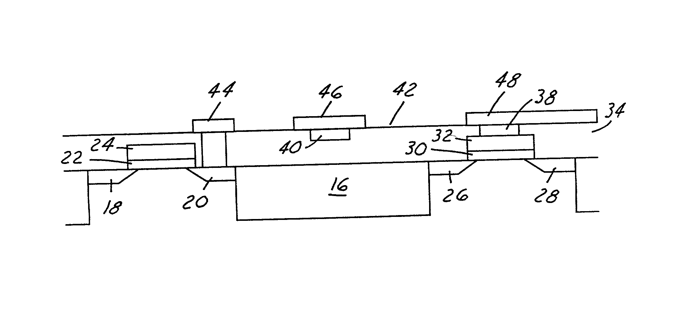
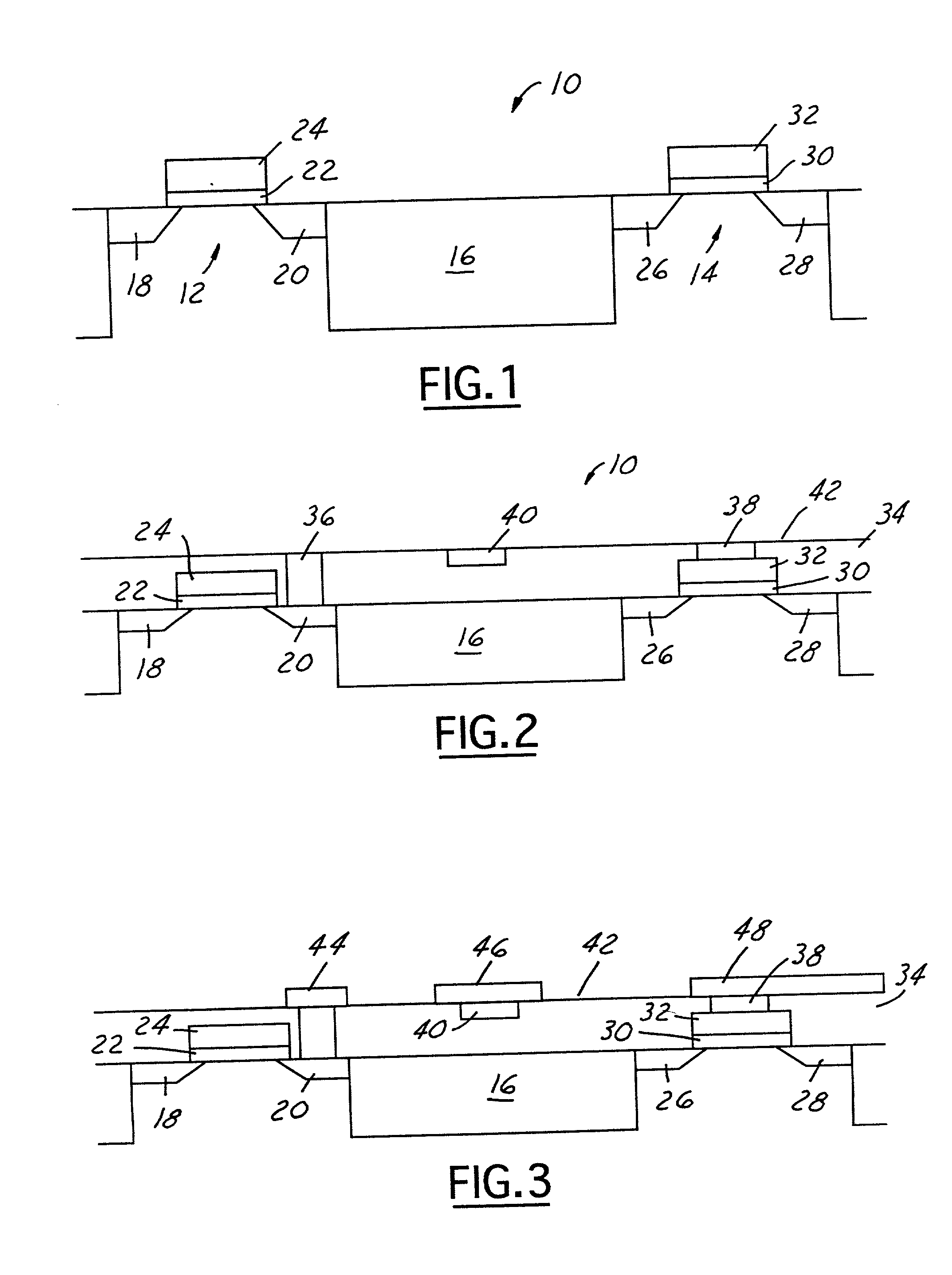
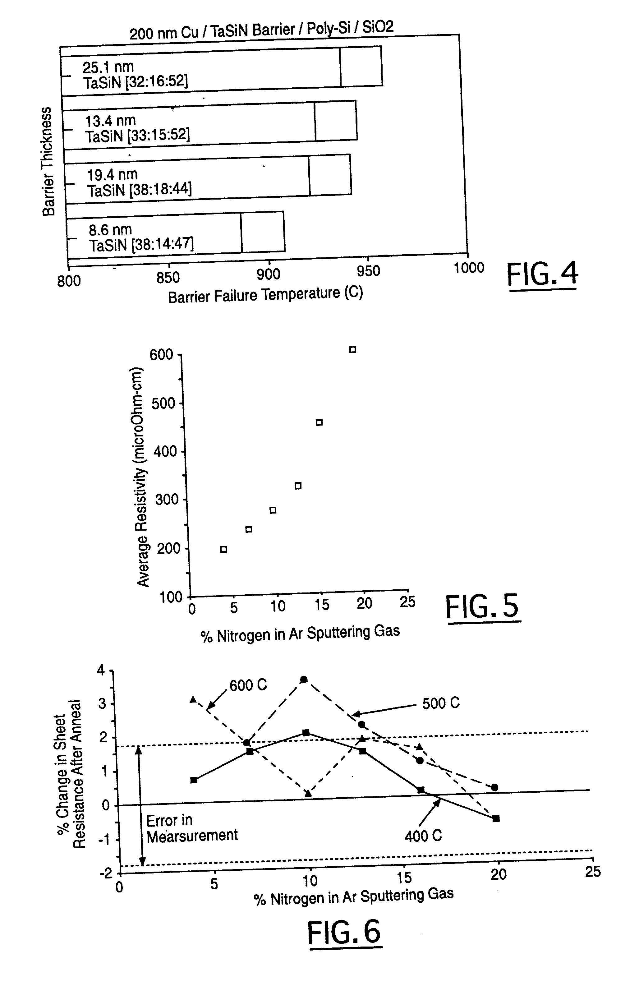
[0039] The present invention discloses a semiconductor structure that includes at least one circuit element selected from the group consisting of a fuse, a diffusion barrier, a resistor, a trimable resistor and a capacitor; the at least one circuit element may be formed of refractory metal-silicon-nitrogen. The structure further includes a pre-processed substrate which may be formed of a semi-conducting material or of an electrically insulating material. The refractory metal in the refractory metal-silicon-nitrogen compound may be selected from the group of elements consisting of Ta, Nb, V, W and Ti. In a typical refractory metal-silicon-nitrogen composition of TaSiN, the composition may contain between about 10 at. % and about 55 at. % Ta, between about 10 at. % and about 45 at. % Si, and between about 30 at. % and about 80 at. % N. The semiconductor structure may also include at least one conductive element that is used to establish an electrical connection with the circuit elemen...


PUM

PropertyMeasurementUnit
timeaaaaaaaaaa
timeaaaaaaaaaa
temperatureaaaaaaaaaa

Abstract

A semiconductor structure that includes at least one circuit element of a fuse, a diffusion barrier or a capacitor that is formed by refractory metal-silicon-nitrogen is disclosed. A method for fabricating such semiconductor structure that includes a fuse element, a diffusion barrier, a resistor or a capacitor by a refractory metal-silicon-nitrogen material is further disclosed. A suitable refractory metal-silicon-nitrogen material to be used is TaSiN which provides a wide range of resistivity by changing the ratio of Ta:Si:N. The invention provides the benefit that the various components of diffusion barriers, fuses, capacitors and resistors may be formed by a single deposition process of a TaSiN layer, the various components are then selectively masked and treated by either heat-treating or ion-implantation to vary their resistivity selectively while keeping the other shielded elements at the same resistivity.

Description

FIELD OF THE INVENTION[0001] The present invention generally relates to a semiconductor device incorporating circuit elements that are formed of refractory metal-silicon-nitrogen and a method for such fabrication and more particularly, relates to a semiconductor device that incorporates circuit elements such as resistors, capacitors, fuses and diffusion barriers that are formed of metal-silicon-nitrogen and method for such fabrication.BACKGROUND OF THE INVENTION[0002] In semiconductor devices, capacitors, fuses and diffusion barriers are frequently formed in-situ in the semiconductor structure, while resistors are typically connected to a circuit board external to the semiconductor structure to provide required electrical resistance to an electronic circuit.[0003] It is therefore difficult to provide resistors that are built in-situ in a semiconductor structure. It is particularly difficult to form in-situ resistors in a semiconductor structure to provide high resistance, i.e. to pr...

Claims


Application Information

Patent Timeline
Patent Type & Authority Applications(United States)
IPC IPC(8): H01L21/02H01L21/768H01L23/525H01L27/06
CPCH01L21/76849H01L21/7687H01L21/76888H01L23/5258H01L27/0629H01L28/24H01L2924/0002H01L2924/00
Inventor CABRAL, CYRIL JR.CLEVENGER, LAWRENCEHSU, LOUIS LU-CHENWONG, KEITH KWONG HON
Owner GLOBALFOUNDRIES INC
Why Eureka
Try Eureka