Electro-chemical machining apparatus

a technology of electrochemical machining and machining equipment, which is applied in the direction of cutting machines, manufacturing tools, edge grinding machines, etc., can solve the problems of increasing wiring electric resistance, significant damage to semiconductor substrates, and problematic wiring electric resistan

Inactive Publication Date: 2002-10-31
SONY CORP
View PDF12 Cites 36 Cited by
  • Summary
  • Abstract
  • Description
  • Claims
  • Application Information

AI Technical Summary

Problems solved by technology

However, the aforementioned copper wiring using the dual damascene process might cause significant damages to the semiconductor substrate because the conventional CMP method for removing excessive copper film 307 and smoothing the surface has a drawback in which the a polishing tool applies pressure onto the copper film.
Especially, in the case where an organic insulation film having low mechanical strength and low dielectric constant as the interlayer insulation film, the abovementioned damages are not negligible because it may result in defects such as cracks in the interlayer insulation film or peeling the interlayer insulation film out of the semiconductor substrate.
The dishing is one of the primary causes of wiring problems due to insufficient cross section area of the wiring 308 leading to increased wiring electric resistance.
If such erosion occurred, a cross section area of the wiring is reduced in such an amount that might result in problematic wiring electric resistance.
Again, cross section area of the wirings is insufficient in this case and might result in wiring electric resistance defects.
However, increased pressure to the polishing tool may result in scratches (SC) or chemical damages (CD) on the surface of wirings, as shown in FIG. 43.
This is most likely to occur in soft copper, thereby causing troubles such as open circuits, short circuits, defective wiring resistance, etc.
Also, increased pressure applied onto the polishing tool may result in increased likelihood of the aforementioned scratches, peeling of the interlayer insulation film, dishing, erosion and recess to occur.

Method used


Image

  • Electro-chemical machining apparatus
  • Electro-chemical machining apparatus
  • Electro-chemical machining apparatus

Examples


first embodiment

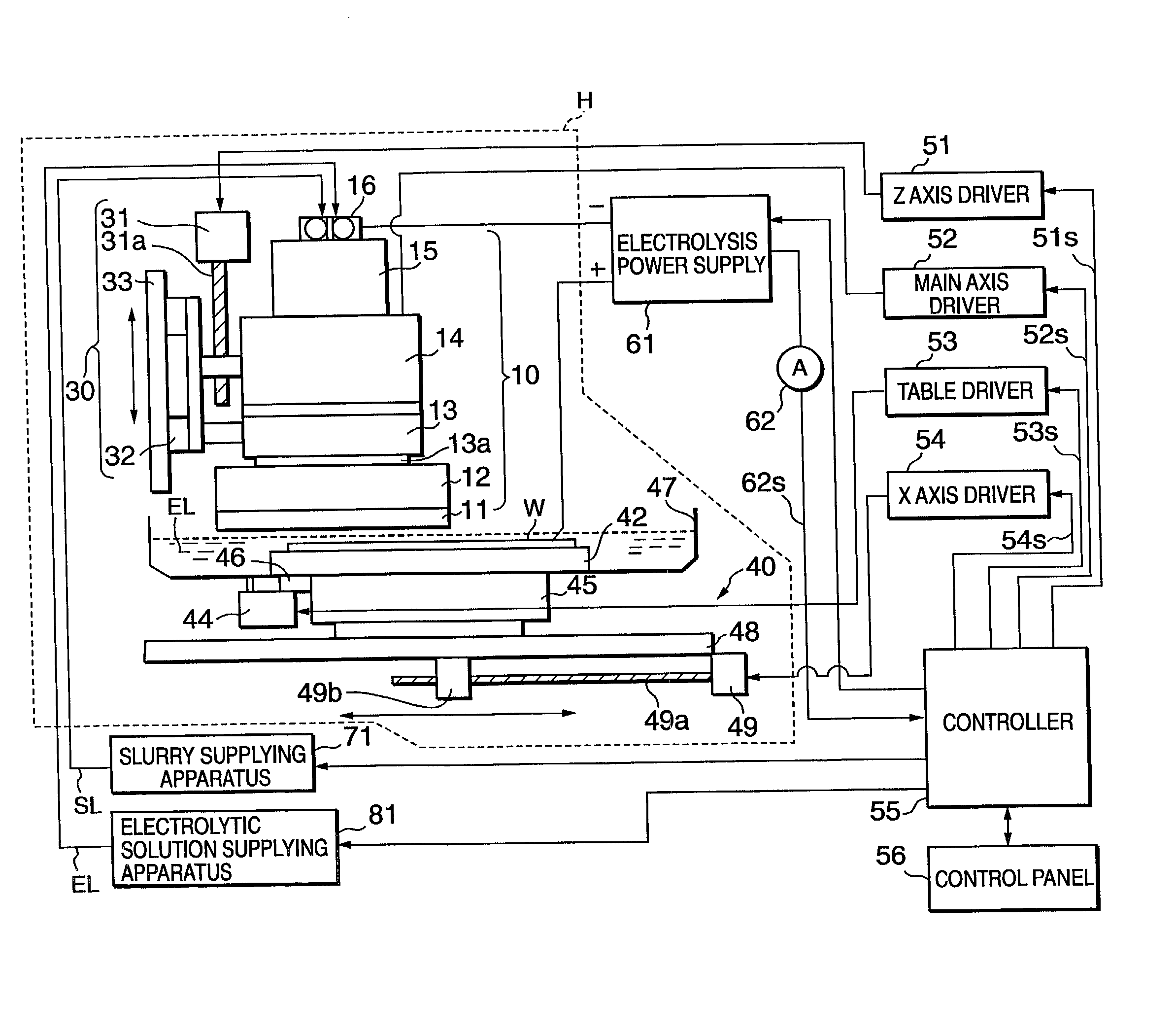
[0178] the electro-chemical machining apparatus according to the present invention will be described by way of an example of applied to metal wiring fabrication steps for semiconductor devices by a dual damascene process.

[0179] Semiconductor device fabrication process applying the electro-chemical machining apparatus according to the present invention will be described hereafter.

[0180] Firstly, as illustrated in FIG. 1, an interlayer insulation layer 102 of, e.g., silicon oxide film is provided on a semiconductor substrate 101 of, e.g., silicon having impurity diffused regions (not shown in FIG. 1). Such interlayer insulation layer 102 is provided by a reduced pressure chemical vapor deposition (CVD) technique using, e.g., TEOS (tetraeethylortheosilicate) as a reaction source. A silicon nitride film and other so-called low-k (low dielectric constant) materials as well as the TEOS film may be used as the interlayer insulation film 102. The low dielectric constant materials include Si...

second embodiment

[0241] (Second Embodiment)

[0242] Illustrated in FIG. 17A is a schematic construction of a main part or portion of the electro-chemical machining apparatus according to the second preferred embodiment of the present invention. The electro-chemical machining apparatus of the second preferred embodiment has essentially a construction which is similar as that of the first preferred embodiment but differs in the provision of a spacer 25 at the machining surface side of the electrode plate 23 acting as the cathode.

[0243] FIG. 17B is a schematic perspective view of the spacer 25 which may comprise a columnar base formed with through-holes 25a for passing the electrolytic solution. In the electro-chemical machining apparatus in this embodiment, the thickness of the spacer 25 is varied in the range of, e.g., several mm to tens of mm to control the distance between the electrode 23 and the surface to be machined of the wafer W In this way, the electrolytic current is adjusted to improve the q...

third embodiment

[0244] (Third Embodiment)

[0245] Illustrated in FIG. 18A is a schematic top view of the wafer, the electrode plate acting as the cathode and a wiper, which are main parts of the electro-chemical machining apparatus of a third preferred embodiment of the present invention. FIG. 18B is a schematic side view corresponding to FIG. 18A.

[0246] Unlike the first and second embodiments, the electro-chemical machining apparatus according to the third preferred embodiment has the electrode plate and the wiper separated from each other. That is, the wafer W is mounted on a rotary wafer table 42 driven to rotate with the surface to be machined facing upwardly. The electrode plate 23 acting as the cathode supported by an electrode support 34 and the wiper 24 supported by a wiper support 35 are disposed in opposite relationship to the surface to be machined of the wafer W.

[0247] In other words, the electrode support 34 rotatably holds the electrode plate 23 in such a manner to rotate the electrode ...


PUM

PropertyMeasurementUnit
temperatureaaaaaaaaaa
depthaaaaaaaaaa
thicknessaaaaaaaaaa

Abstract

The electro-chemical machining apparatus of this invention is designed to smoothing a metal film by efficiently reducing initial rough surface and removing excessive metal film with reduced damages to the metal film. For this end, the electro-chemical machining apparatus performs electro-chemical machining of an object to be machined having a metal film on the surface to be machined. Such apparatus has a means for holding the object to be machined, a wiper for wiping the surface of the object to be machined, a means for supplying electrolytic solution onto the surface of the object to be machined, a first electrode disposed at a position opposed to the surface of the object to be machined, a second electrode disposed at a peripheral portion on the surface of the object to be machined, and a power supply for causing electrical current to flow between the second electrode on the surface of the object to be machined and the first electrode.

Description

[0001] This application claims priority to Japanese Patent Application No. JP 2001-056027, filed on Feb. 28, 2001, and the disclosure of such application is herein incorporated by reference to the extent permitted by law.[0002] 1. Field of the Invention[0003] The present invention is related to an electro-chemical machining apparatus, more specifically to an electro-chemical machining apparatus for smoothing a rough surface on a metal film forming process.[0004] 2. Related Art[0005] High scale integration and miniaturization of semiconductor devices have accelerated the introduction of narrower, fine pitch and multilayered wirings, thus increasing the significance of multilayer wiring techniques in semiconductor fabrication processes.[0006] Although it has been conventional to use aluminum as wiring material in multilayer semiconductor devices, many attempts have been made to develop new wiring processes replacing aluminum with copper as the wiring material so as to reduce signal pr...

Claims


Application Information

Patent Timeline
Patent Type & Authority Applications(United States)
IPC IPC(8): B24B7/22B24B21/04B23H3/00B24B37/04B24B57/02C25F7/00H01L21/3205H01L21/321H01L21/768
CPCB24B7/228B24B21/04Y10S451/908B24B57/02B24B37/04
Inventor SATO, SHUZOYASUDA, ZENYAISHIHARA, MASAOOOTORII, HIIZUNOGAMI, TAKESHIKOMAI, NAOKI
Owner SONY CORP
Why Eureka
Try Eureka