

Light emitting device and method of manufacturing thereof
a technology of light emitting devices and manufacturing methods, applied in the direction of luminescent compositions, identification means, instruments, etc., can solve the problems of high cost of organic compound materials generally used in light emitting elements, low cost, and ideal film formation methods
- Summary
- Abstract
- Description
- Claims
- Application Information
AI Technical Summary
Benefits of technology
Problems solved by technology
Method used
Image

Examples
embodiment
[0067] [Embodiment 1]
[0068] A method of manufacturing a pixel portion of a light emitting device is explained in Embodiment 1 using FIGS. 3A to 4C. Further, a case of forming a thin film transistor (TFT) as a semiconductor element is explained in Embodiment 1.
[0069] First, a crystalline semiconductor film having a film thickness of 50 nm is formed on a transparent substrate 301. Note that a known means may be used as the method of forming the crystalline semiconductor film. The crystalline semiconductor film is patterned next, forming semiconductor layers 302 and 303 (hereafter referred to as active layers) made from island-shape crystalline semiconductor films. A gate insulating film 304 is then formed from a silicon oxide film, covering the active layers 302 and 303. Gate electrodes 305 and 306 are formed next on the gate insulating film 304. (See FIG. 3A.) An element selected from the group consisting of Ta, W, Ti, Mo, Al, and Cu, or an alloy or a compound material having one of ...
embodiment 2
[0093] [Embodiment 2]
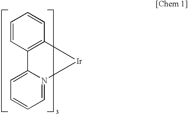
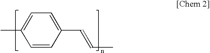
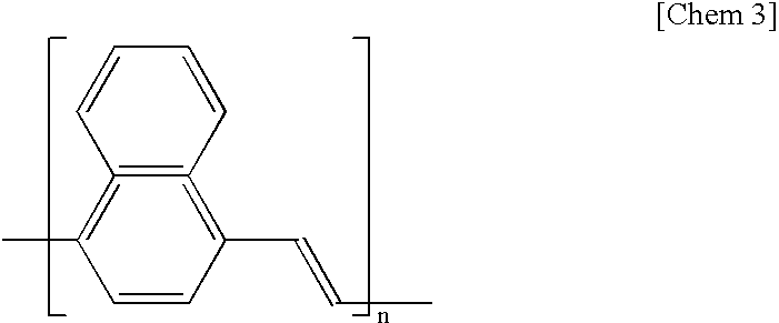
[0094] An example is shown in Embodiment 1 of using an iridium complex, a low molecular weight material, as an organic compound, but it is also possible to use high molecular weight materials in light emitting layers, as shown below. Note that, except for the organic compound layer, the structure in Embodiment 2 is identical to that of Embodiment 1, and for simplicity a detailed explanation of the identical portions is omitted here. In addition, the same reference numerals in FIGS. 3A to 4C are used in this explanation for portions that are identical to those of Embodiment 1.
[0095] Processing is first performed in accordance with Embodiment 1 until immediately before formation of the organic compound layer.
[0096] Next, a hole injecting layer 524 is formed on the anode 322 by the method shown in the embodiment mode. A composition in which a material referred to as PEDOT (poly(3,4-ethylene dioxythiophene)) is dissolved by polystyrene sulfonic acid (referred to as ...
embodiment 3
[0110] [Embodiment 3]
[0111] An example of using a low molecular weight iridium complex as an organic compound is shown in Embodiment 1. However, in the present invention, it is also possible to use other molecular materials in light emitting layers as shown below.
[0112] It is possible to use a material referred to as quinacridon as a substitute for the iridium complex of Embodiment 1. The molecular formula of quinacridon is shown below. 9
[0113] Further, it is also possible to use a material referred to as BCP, basocuproin. as a substitute for the iridium complex of Embodiment 1. Its molecular formula is shown below. 10
[0114] Furthermore, the aforementioned materials may also be used in combination of two, three, or more.
[0115] Note that the above materials are not soluble in toluene or in alcohols.
PUM
| Property | Measurement | Unit |
|---|---|---|
| temperature | aaaaa | aaaaa |
| thickness | aaaaa | aaaaa |
| thickness | aaaaa | aaaaa |
Abstract
Description
Claims
Application Information