Light emitting device

a technology of light-emitting devices and semiconductors, which is applied in the direction of semiconductor devices, electrical equipment, transistors, etc., can solve the problems of low electric field effect mobility of tft using amorphous silicon, inability to operate at the frequency required to process video signals, and limit in a system for mounting drivers i

Inactive Publication Date: 2003-02-06
SEMICON ENERGY LAB CO LTD
View PDF19 Cites 86 Cited by
  • Summary
  • Abstract
  • Description
  • Claims
  • Application Information

AI Technical Summary

Problems solved by technology

However, the TFT using amorphous silicon is low in electric field effect mobility, and cannot be operated at a frequency required to process the video signal.
Accordingly, it is considered that there is a limit in a system for mounting the driver IC.
An increase in the connecting terminal number causes an increase in generating probability of a contact defect.
Further, it becomes a factor in which the area (trim area) of a peripheral portion of a pixel section is increased and the compactness of a semiconductor device with this pixel section as a display and the design of an external appearance are damaged.
However, even when the TFT was formed by using the polycrystal silicon, its electrical characteristics were finally not equivalent to the characteristics of a MOS transistor formed in a monocrystal silicon substrate.
Further, a problem exists in that an off-electric current is raised by a defect formed in a crystal grain boundary.
However, when the structure of the TFT is optimized to obtain characteristics required in the pixel section and each driving circuit, the number of photo masks is increased so that a manufacturing process becomes complicated and a process number is necessarily increased.

Method used


Image

  • Light emitting device
  • Light emitting device
  • Light emitting device

Examples


embodiment 1

[0083] (Embodiment 1)

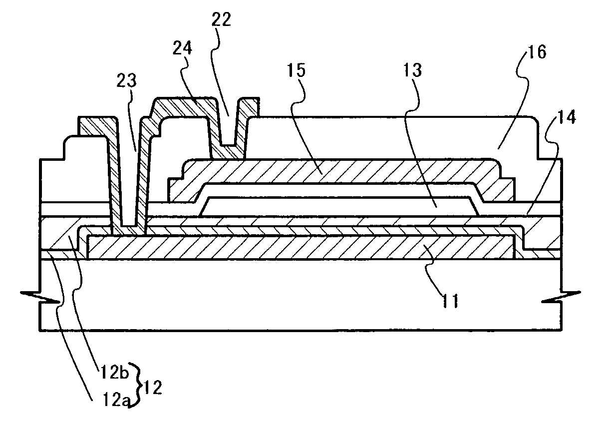
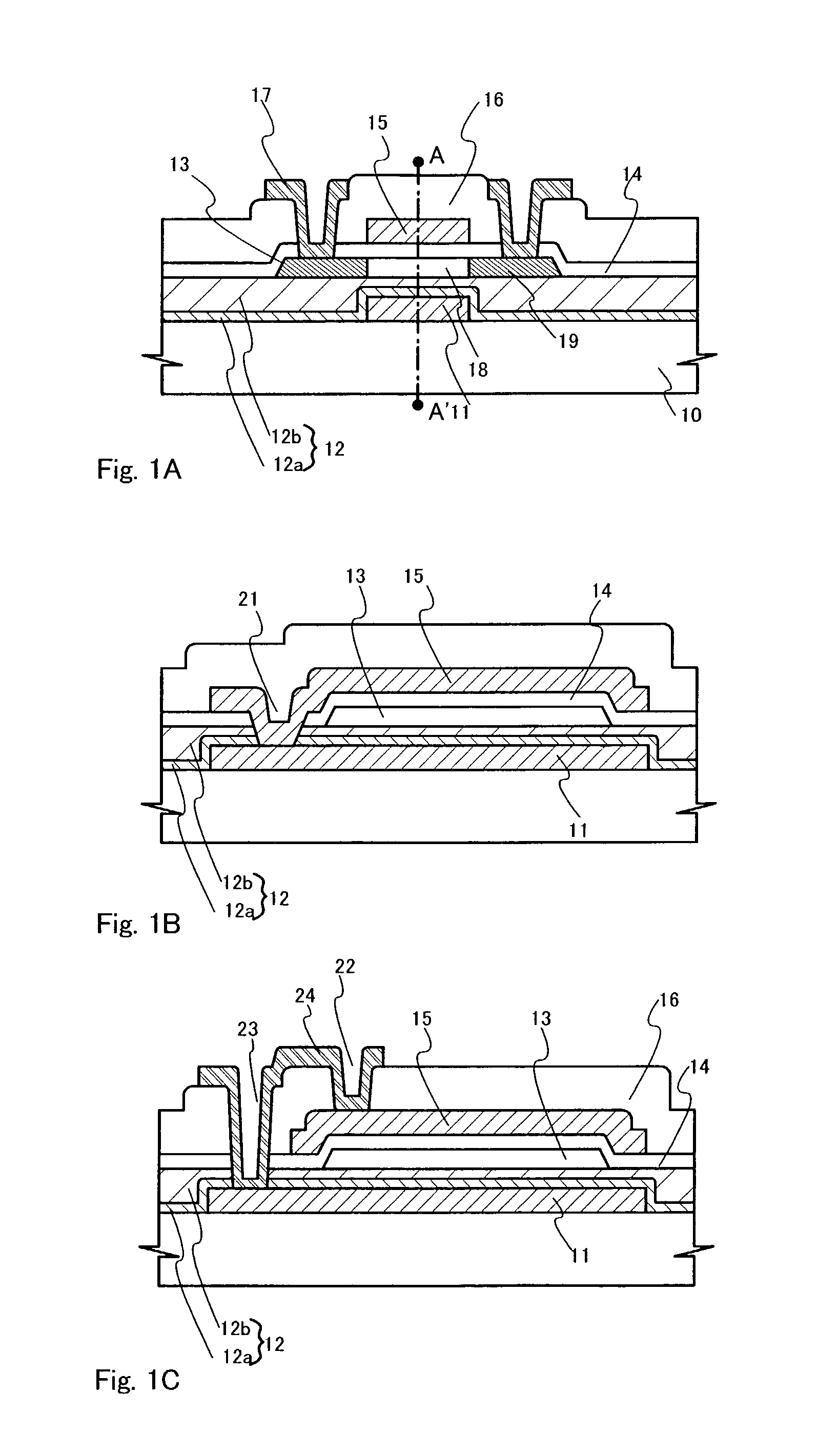
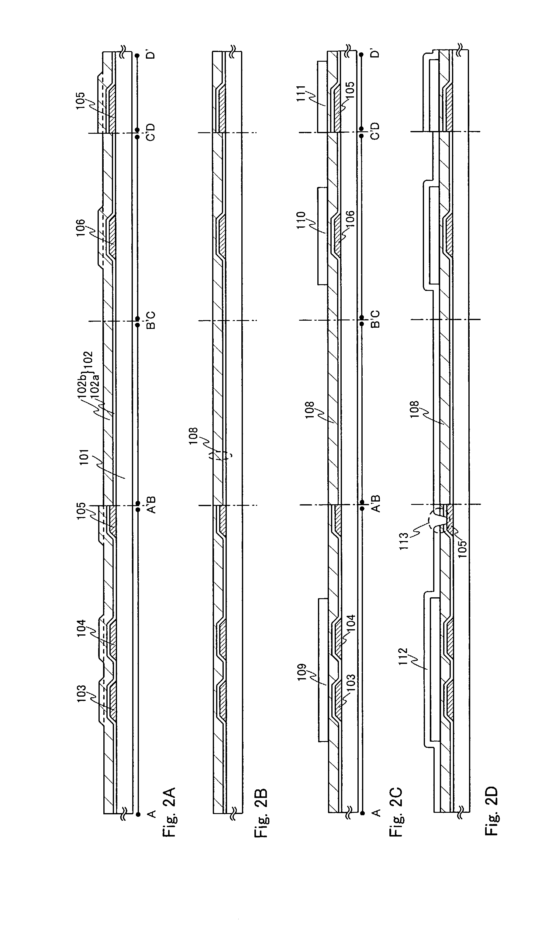
[0084] In this embodiment, steps of manufacturing a semiconductor device according to the present invention will be described. In addition, a method of manufacturing TFT's for a pixel section will be described in detail here. Note that, this embodiment shows an example that a common voltage is applied to a first electrode on TFT used as a switching element (switching TFT) and the first electrode and a second electrode are connected to each other on TFT controlling current which flows to the light emitting element (driving TFT). Further, although the method of manufacturing TFT's for the pixel section is only described in this embodiment, TFT's for a driver circuit may also be manufactured simultaneously.

[0085] FIGS. 2 to 5 are cross-sectional views for explaining the semiconductor device manufacturing steps. FIGS. 6 to 8 are corresponding top views. For the convenience of explanation, common reference symbols are used therein.

[0086] In FIG. 2A, a substrate made ...

embodiment 2

[0127] (Embodiment 2)

[0128] In this embodiment, the construction of a pixel of the light emitting device of the present invention different from that in the embodiment 1 will be explained.

[0129] FIG. 9 shows a top view of the pixel of the light emitting device of this embodiment. FIG. 10 shows a sectional view in A-A', B-B' and C-C' of FIG. 9. A partition wall layer, an organic light emitting layer, a cathode and a protecting film manufactured in the process subsequent to the formation of a pixel electrode are omitted to clarify the construction of the pixel in FIG. 9.

[0130] Reference numeral 301 designates a TFT for switching, and an n-channel TFT is used in this embodiment. Reference numeral 302 designates a TFT for driving, and a p-channel TFT is used in this embodiment. The TFT for switching and the TFT for driving may be set to the n-channel TFT and the p-channel TUT.

[0131] The TFT 301 for switching has first electrodes 306, 307, a first insulating film 350 abutting on the firs...

embodiment 3

[0145] (Embodiment 3)

[0146] In this embodiment, the construction of a pixel of the light emitting device of the present invention different from that in the embodiments 1, 2 will be explained.

[0147] FIG. 11 shows a top view of the pixel of the light emitting device of this embodiment. FIG. 12 shows a sectional view in A-A', B-B', C-C' and D-D' of FIG. 11. A partition wall layer, an organic light emitting layer, a cathode and a protecting film manufactured in the process subsequent to the formation of a pixel electrode are omitted to clarify the construction of the pixel in FIG. 11.

[0148] Reference numeral 401 designates a TFT for switching, and an n-channel TFT is used in this embodiment. Reference numeral 402 designates a TFT for driving, and a p-channel TFT is used in this embodiment. The TFT for switching and the TFT for driving may be also set to the n-channel TFT and the p-channel TFT.

[0149] The TFT 401 for switching has first electrodes 406, 407, a first insulating film 450 ab...


PUM


Abstract

An object of the invention is to provide a technique for improving the characteristics of a TFT and realizing an optimum structure of the TFT for the driving conditions of a pixel section and a driving circuit by a small number of photo masks. Therefore, a light emitting device has a semiconductor film, a first electrode and a first insulating film nipped between the semiconductor film and the first electrode. Further, the light emitting device has a second electrode and a second insulating film nipped between the semiconductor film and the second electrode. The first and second electrodes are overlapped with each other through a channel forming area arranged in the semiconductor film. In the case of a TFT in which a reduction in off-electric current is considered important in comparison with an increase in on-electric current, a constant voltage (common voltage) is applied to the first electrode at any time. In the case of a TFT in which the increase in on-electric current is considered important in comparison with the reduction in off-electric current, the same voltage is applied to the first and second electrodes.

Description

[0001] 1. Field of the Invention[0002] Present invention relates to the manufacturing method of semiconductor device, in particular, present invention relates to a light emitting device comprising a light emitting element (OLED: Organic Light Emitting Device) formed on a plastic substrate. The invention also relates to an OLED module in which an IC's including a controller, or the like, is mounted on the OLED panel. Note that, in this specification, light emitting device is the generic term for the OLED panel and for the OLED module. Electronic equipment using the light emitting device is also included in the present invention.[0003] 2. Description of the Related Art[0004] Recently, technology for forming TFTs (Thin Film Transistor) on a substrate has greatly progressed, and its application to an active matrix display device is actively developed. In particular, TFTs using a polysilicon film have higher field effect mobility (also referred to as mobility) than that of conventional T...

Claims


Application Information

Patent Timeline
Patent Type & Authority Applications(United States)
IPC IPC(8): H01L21/336H01L21/77H01L21/84H01L27/12H01L29/786
CPCH01L21/3226H01L27/3244H01L29/6675H01L29/66757H01L29/78603H01L27/1288H01L29/78645H01L29/78648H01L29/78696H01L27/124H01L29/78636H10K59/1213H10K59/131
Inventor YAMAZAKI, SHUNPEIKOYAMA, JUN
Owner SEMICON ENERGY LAB CO LTD
Why Eureka
Try Eureka