TFT array substrate and active-matrix addressing liquid-crystal display device

a liquid crystal display and active matrix technology, applied in semiconductor devices, instruments, optics, etc., can solve the problems of large current leakage, large current leakage, and inducible current leakag

Inactive Publication Date: 2003-02-06
GOLD CHARM LTD
View PDF1 Cites 45 Cited by
  • Summary
  • Abstract
  • Description
  • Claims
  • Application Information

AI Technical Summary

Problems solved by technology

If light is irradiated to the active layer, current leakage will be induced due to optical excitation.
On the other hand, as described previously, high-luminance light is inputted into the LCD device for the light bulb and thus, the current leakage will be large.
Since, in addition to the light from the source, the reflected light by the projection light system is irradiated to the active layer, the current leakage is likely to be larger.
From this point of view, the above-described problem about the current leakage will be more serious.
However, there is a problem that the light entering from the side of the substrate 100 is unable to prevent sufficiently from being irradiated to the LDD regions 107b and 107b and/or the channel region 107c of the TFT 131.
This leads to a disadvantage that the aperture ratio is unable to be increased.
Thus, optically induced current leakage increases and as a result, a problem of degradation of contrast and non-uniformity of image quality occurs.
Therefore, there is a problem that the fabrication processes are complicated.
Therefore, there is a problem that the fabrication processes a...

Method used


Image

  • TFT array substrate and active-matrix addressing liquid-crystal display device
  • TFT array substrate and active-matrix addressing liquid-crystal display device
  • TFT array substrate and active-matrix addressing liquid-crystal display device

Examples


first embodiment

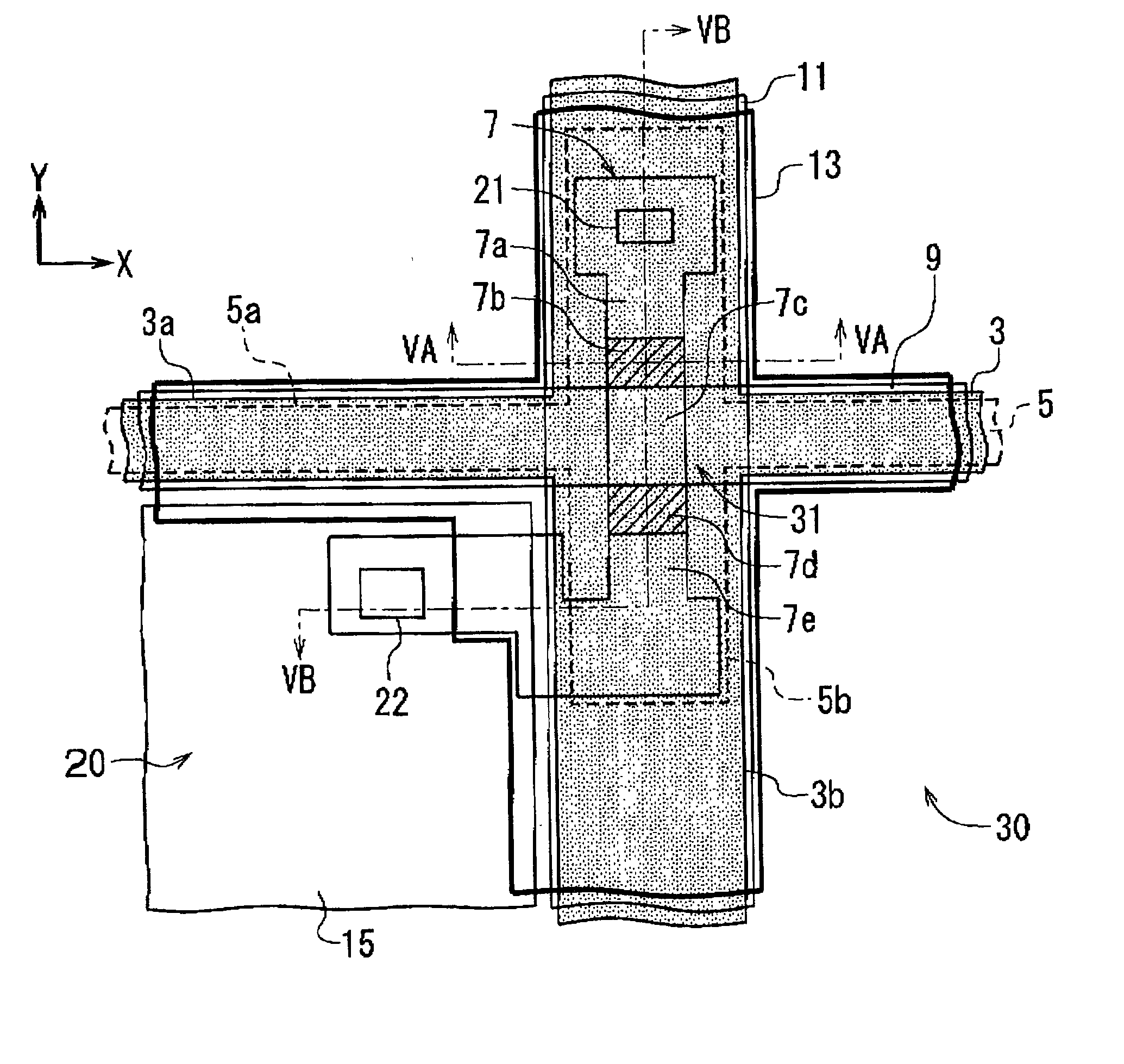
[0132] FIG. 4 and FIGS. 5A and 5B show the schematic configuration of a TFT array substrate 30 according to a first embodiment of the invention, in which only one pixel is illustrated for simplification. This is applicable to any other embodiments explained later.

[0133] The TFT array substrate 30 comprises a transparent plate 1, on which TFTs 31 are arranged in a matrix array. The plate 1 is made of transparent and dielectric material such as glass.

[0134] A SiO.sub.2 layer 2 is formed on the plate 1 to cover its whole surface. This layer 2 is to prevent heavy metals contained in the plate 1 from diffusing into the inside of the substrate 30.

[0135] A patterned first light-shielding layer 3 is formed on the SiO.sub.2 layer 2. The plan shape of the layer 3 is like a lattice, which is formed by lateral strips 3a extending along the rows (the X direction in FIG. 4) of the matrix of the TFTs 31 and vertical strips 3b extending along the columns (the Y direction in FIG. 4) thereof and inte...

second embodiment

[0171] FIGS. 12 and 13A to 13B show the structure of a TFT array substrate 30A according to a second embodiment of the invention, in which only one pixel is illustrated for simplification.

[0172] The substrate 30A of the second embodiment has the same configuration as the substrate 30 of the first embodiment, except that a second light-shielding layer 5A has conductivity and electrically connected to the corresponding gate lines 9. Therefore, the explanation about the same configuration is omitted here for the sake of simplification by attaching the same reference symbols as used in the first embodiment of FIGS. 4 and 5A to 5B to the same or corresponding elements in the second embodiment of FIGS. 12 and 13A and 13B.

[0173] In the substrate 30A, the second light-shielding layer 5A, which is made of an impurity-doped polysilicon, is formed on the SiO.sub.2 layer 4. The layer 5A has strip-shaped first parts 5Aa extending along the rows of the matrix (i.e., in the X direction) and rectan...

third embodiment

[0180] FIGS. 14 and 15A to 15B show the structure of a TFT array substrate 30B according to a third embodiment of the invention, in which only one pixel is illustrated for simplification.

[0181] The substrate 30B of the third embodiment has the same configuration as the substrate 30 of the first embodiment, except that a second light-shielding layer 5B has conductivity and is applied with a constant voltage v.sub.c. Therefore, the explanation about the same configuration is omitted here for the sake of simplification by attaching the same reference symbols as used in the first embodiment of FIGS. 4 and 5A to 5B to the same or corresponding elements in the second embodiment of FIGS. 14 and 15A and 15B.

[0182] In the substrate 30B, the second light-shielding layer 5B, which is made of an impurity-doped polysilicon is formed on the SiO.sub.2 layer 4. The layer 5B has strip-shaped first parts 5Ba extending along the rows of the matrix (i.e., in the X direction) and strip-shaped second par...


PUM


Abstract

A TFT array substrate is provided, which blocks effectively the light traveling toward the active layers of the TFTs. A patterned first light-shielding layer is formed between a transparent plate and TFTs in such a way as to overlap with the active layers of the TFTs. A patterned third light-shielding layer is formed to cover the TFTs on the opposite side to the plate with respect to the TFTs. The third light-shielding layer has the first parts extending along the rows of the matrix and the second parts extending along the columns thereof. A patterned second light-shielding layer is formed between the first light-shielding layer and the TFTs. The second light-shielding layer has a light-absorbing property, which absorbs the light entering the inside of the substrate. A patterned fourth light-shielding layer, which has a light-absorbing property, may be additionally provided between the TFTs and the third light-shielding layer.

Description

[0001] 1. Field of the Invention[0002] The present invention relates generally to Liquid-Crystal Display (LCD) devices. More particularly, the invention relates to a substrate on which Thin-Film Transistors (TETs) are arranged in a matrix array, i.e., a TFT array substrate, and an active-matrix addressing LCD device equipped with the substrate. This substrate and device are preferably applicable to the light bulb of the projection type display device.[0003] 2. Description of the Related Art[0004] In recent years, various types of display devices applicable to wall-hung type televisions (TVs), projection type TVs, or Office Automation (OA) equipment have been developed. To realize high-grade display devices for OA equipment or high-definition TVs (HDTVs), active-matrix addressing LCD devices utilizing TFTs as their switching elements are more promising within the conventional display devices. This is because active-matrix LCD devices have an advantage that contrast and response speed...

Claims


Application Information

Patent Timeline
IPC IPC(8): G02F1/1362
CPCG02F1/136209G02F1/136227H01L27/12H01L29/78633
Inventor SERA, KENJIOKUMURA, FUJIO
Owner GOLD CHARM LTD
Why Eureka
Try Eureka