

Illumination system particularly for microlithography
a technology of illumination system and microlithography, which is applied in the direction of photomechanical equipment, instruments, optical radiation measurement, etc., can solve the problems of the optical components of the collector unit and and achieve the effect of reducing the diameter of the light beam
- Summary
- Abstract
- Description
- Claims
- Application Information
AI Technical Summary
Benefits of technology
Problems solved by technology
Method used
Image

Examples
first embodiment
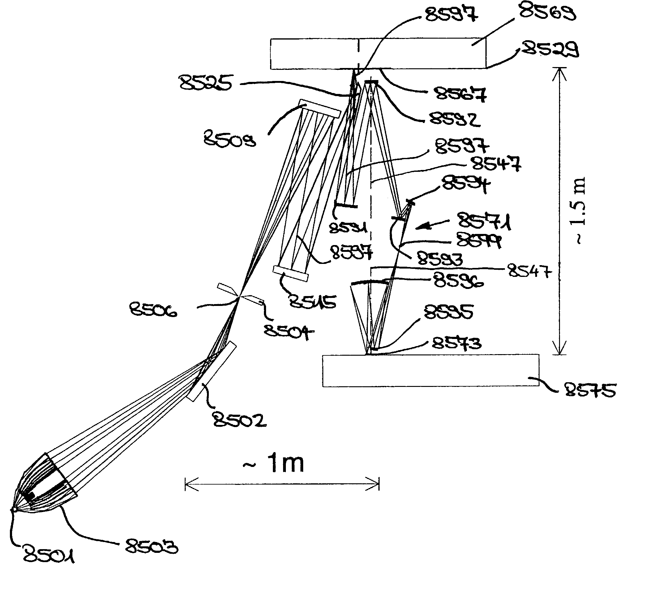
[0352] In FIG. 85 an inventive projection exposure apparatus is shown. Corresponding elements have the same reference numbers as those in FIG. 84 increased by 100.
[0353] The first embodiment comprises a primary light source 8501 and a collecting optical element a so-called collector 8503. The collector 8503 is a nested grazing incidence collector as shown, for example, in WO 02 / 27400 A2. The radiation is spectral filtered by grating element 8502 together with aperture stop 8504. The grating element diffracts the light impinging onto the grating element in different diffraction orders, e.g., the -1.diffration order. The aperture stop 8504 is situated in or nearby an intermediate image 8506 of the primary light source in the -1.diffraction order. The projection exposure apparatus further comprises a first optical component having a first optical element with first or so called field raster elements 8509 and a second optical element with second or so called pupil raster elements 8515. ...
second embodiment
[0360] In FIG. 87 the invention is shown. Corresponding elements have the same reference numbers as those in FIG. 85 increased by 200. The difference between the embodiment shown in FIG. 85 and the embodiment shown in FIG. 87 is the field forming of the arc-shaped field in the image plane. According to the embodiment shown in FIG. 87 no field-forming mirror is necessary any longer. Therefore the system shown in FIG. 87 is most compact in size and furthermore, has, due to fewer optical elements in respect to a projection exposure apparatus shown, for example, in FIG. 84, a high transmission of light entering the projection exposure apparatus.
[0361] The field according to the embodiment shown in FIG. 87 is formed by the first raster elements 8709, which have the shape of the field to be illuminated in the image plane 8729. For an arc-shaped field in the image plane 8729, the field raster elements or first raster elements have an arcuate shape.
[0362] The real entrance pupil 8788 of the...
PUM
| Property | Measurement | Unit |
|---|---|---|
| wavelengths | aaaaa | aaaaa |
| wavelengths | aaaaa | aaaaa |
| wavelengths | aaaaa | aaaaa |
Abstract
Description
Claims
Application Information