Method for forming pattern using argon fluoride photolithography

a technology of argon fluoride and photolithography, which is applied in the field of forming patterns using argon fluoride photolithography, can solve the problems of difficult control of the process, difficult to obtain a pattern size less than 0.1 .mu.m, and difficult to improve the properties of the material

Inactive Publication Date: 2003-06-19
SK HYNIX INC
View PDF5 Cites 7 Cited by
  • Summary
  • Abstract
  • Description
  • Claims
  • Application Information

AI Technical Summary

Benefits of technology

0013] A method for forming a photoresist pattern with ArF photolithography is disclos...

Problems solved by technology

However, although other various techniques are combined together to improve resolution of the new DUV photo etching technique, it is difficult to obtain a pattern size less than 0.1 .mu.m.
The DUV photo-etching technique is superior in an i-line resolution and depth of focus(DOF), however, it is difficult to control the process.
This problem results from an optical aspect caused by using a short wavelength and a chemical aspect caused by using a chemical amplification type resist.
However, there are several problems with respect to reaction mechanisms in post exposure delay (PED) safety, a substrate dependence and so forth.
It is, however, difficult to improve properties of the material since a benzene ring cannot be used.
However, if...

Method used


Image

  • Method for forming pattern using argon fluoride photolithography
  • Method for forming pattern using argon fluoride photolithography
  • Method for forming pattern using argon fluoride photolithography

Examples


Embodiment Construction

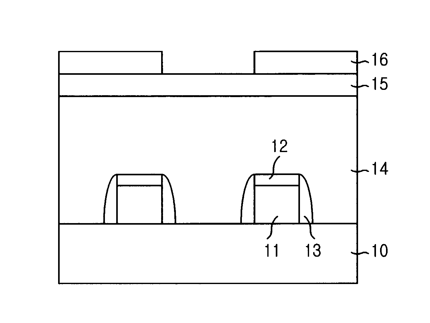
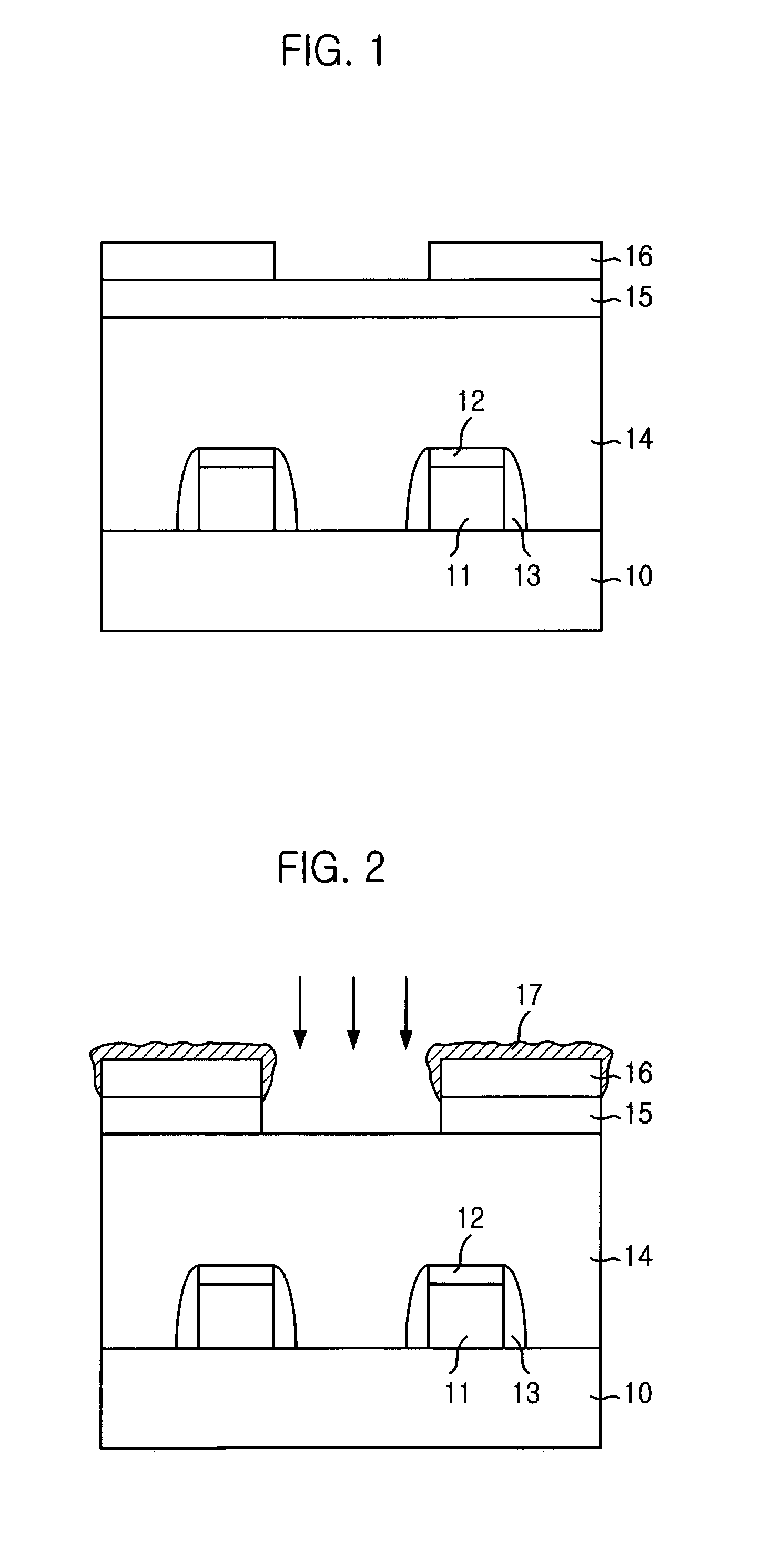
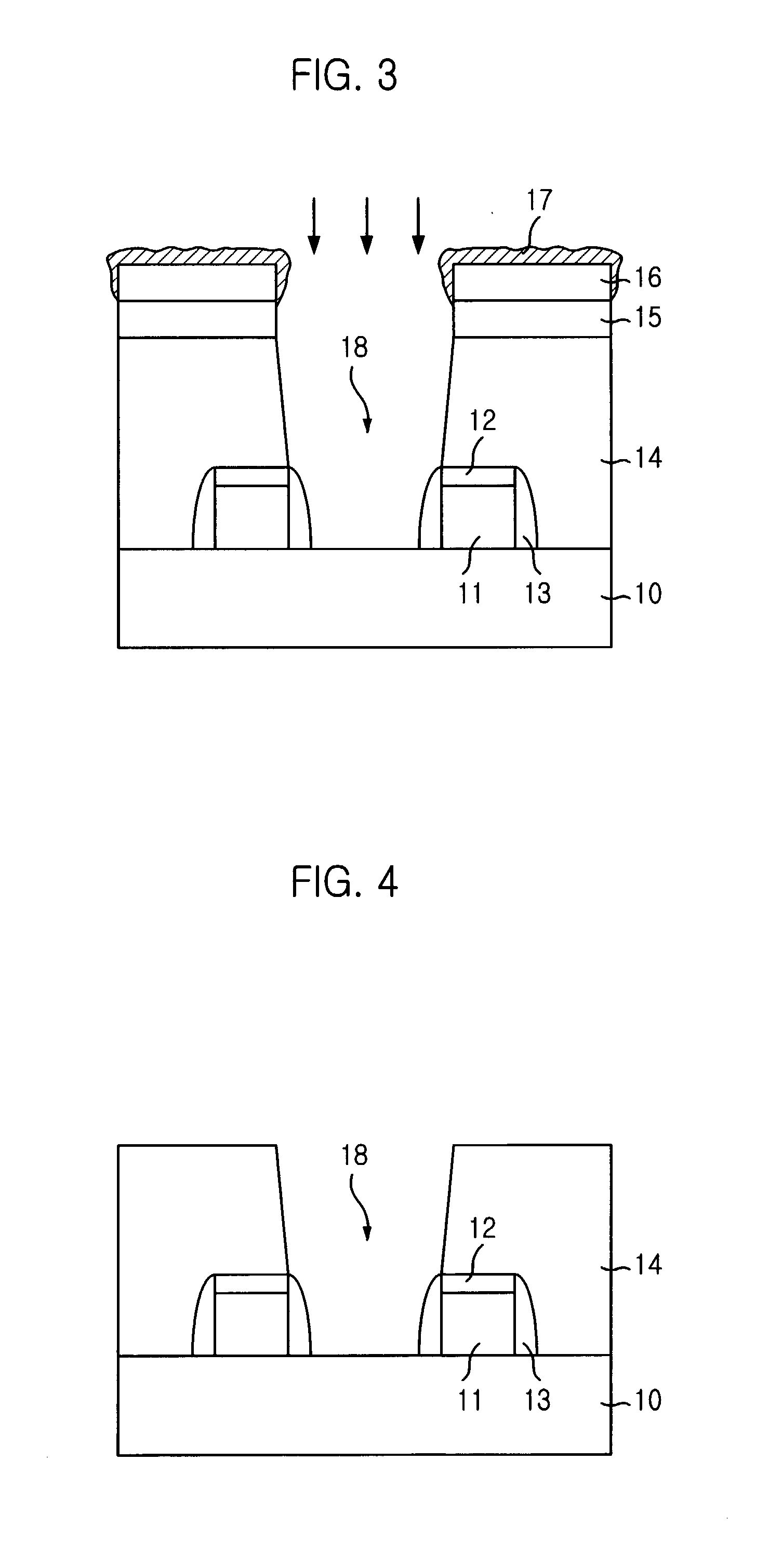
[0016] With reference to FIGS. 1 to 4, the preferred embodiment will be described in more detail.

[0017] Referring to FIG. 1, a number of conductive patterns such as gate electrodes 11 are formed on a substrate 10 including various constructional elements. Instead of the gate electrode 11, a bit line or a metal line having multi-layer structure can be formed.

[0018] That is, a gate oxide layer (not shown) is formed on an interface between the substrate 10 and the gate electrode 11. The gate electrode 11 is formed with stacked layers such as a polysilicon layer / a tungsten silicide layer, or a polysilicon layer / a tungsten layer. A hard mask 12 is formed with a nitride film on the gate electrode 11 for preventing losses of the gate electrode 11 due to a subsequent self align contact (hereinafter referred as to SAC) etching process.

[0019] Subsequently, an insulating layer for a spacer is deposited on a whole surface of the substrate 10 including the gate electrode 11 and the hard mask 12....


PUM

PropertyMeasurementUnit
Pressureaaaaaaaaaa
Pressureaaaaaaaaaa
Pressureaaaaaaaaaa

Abstract

A method for forming a photoresist pattern with minimally reduced transformations through the use of ArF photolithography, including the steps of: forming an organic anti-reflective coating layer on a an etch-target layer already formed on a substrate; coating a photoresist for ArF on the organic anti-reflective coating layer; exposing the photoresist with ArF laser; forming a first photoresist pattern by developing the photoresist, wherein portions of the organic anti-reflective coating layer are revealed; etching the organic anti-reflective coating layer with the first photoresist pattern as an etch mask and forming a second photoresist pattern by attaching polymer to the first photoresist pattern, wherein the polymer is generated during etching the organic anti-reflection coating layer with an etchant including O2 plasma; and etching the etch-target layer by using the second photoresist pattern as an etch mask.

Description

[0001] A method for fabricating a semiconductor device and, more particularly, a method for forming a photoresist pattern using ArF photolithography is disclosed.DESCRIPTION OF THE RELATED ART[0002] Photolithography technology contributes to progression of a semiconductor device development. Thus, improving the resolution of photolithography techniques is critical and directly related to further progression in integration of semiconductor devices.[0003] Currently, photo-etching processes include a process for forming a photoresist pattern and a process for forming a pattern in a preferred form, e.g., a contact hole by etching a etch-target layer through an etching process with use of the photoresist pattern as an etching mask. The photoresist pattern is formed through a series of processes in an order as the following: a process for coating a photoresist on a etch-target layer; a photo exposure process for exposing the photoresist with a mask; and a process for developing the photor...

Claims


Application Information

Patent Timeline
IPC IPC(8): G03F7/00G03F7/40G03F7/11H01L21/027H01L21/3065H01L21/311H01L21/60H01L21/768
CPCH01L21/0275H01L21/31138H01L21/31144Y10S438/952H01L21/76897Y10S438/909H01L21/76802G03F7/00
Inventor LEE, SUNG-KWONKIM, SANG-IKSUH, WEON-JOON
Owner SK HYNIX INC
Why Eureka
Try Eureka