
Board for mounting BGA semiconductor chip thereon, semiconductor device, and methods of fabricating such board and semiconductor device

a technology of bga semiconductor chips and semiconductor devices, which is applied in the manufacture of printed circuits, printed circuit aspects, basic electric elements, etc., can solve problems such as solder failures, reducing the reliability of connections over a long period, and affecting the reliability of connections

Inactive Publication Date: 2003-08-21
NEC TOPPAN CIRCUIT SOLUTIONS
View PDF1 Cites 60 Cited by
  • Summary
  • Abstract
  • Description
  • Claims
  • Application Information

AI Technical Summary

Problems solved by technology

Therefore, the glass epoxy multilayer wiring board is disadvantageous in that when heated, it is warped or distorted, presenting an obstacle to efforts to form fine interconnections in the fabrication of wiring boards and possibly reducing the reliability of connections over a long period of time after components have been mounted on the board.
When solder balls 35 are subjected to reflow heating, solder balls 35 may possibly move due to different flux quantities and different flux activity levels on BGA pad 31, resulting in soldering failures such that adjacent solder balls 35 may join each other and fall off BGA pad 31.
The bonding between BGA pad 31 and solder balls 35 may possibly become unreliable owing to the difference between the coefficient of thermal expansion of the semiconductor device and the coefficient of thermal expansion of the board on which the semiconductor device is mounted.
Particularly, BGA package semiconductor devices of more pins and greater outer profiles tend to have smaller solder bonding strength and suffer more solder joint cracking.
However, since solder ball 35 is not held stably in position but is liable to move in the reflow process, the productivity of the solder ball mounting process is low.
Though the bonding strength of solder ball 35 is high, the BGA pad 31 and insulating layer 33 are not held in intimate contact with each other, with the result that the productivity of the solder ball mounting process is poor.
The laminated assembly of such different materials suffers a strain caused by stresses.
Specifically, since strains concentrate on the corners of the interface between layers 33, 36, the assembly tends to cause fractures such as cracking due to shocks imposed when the assembly falls by gravity and hits a hard object or thermal shocks.

Method used


Image

  • Board for mounting BGA semiconductor chip thereon, semiconductor device, and methods of fabricating such board and semiconductor device
  • Board for mounting BGA semiconductor chip thereon, semiconductor device, and methods of fabricating such board and semiconductor device
  • Board for mounting BGA semiconductor chip thereon, semiconductor device, and methods of fabricating such board and semiconductor device

Examples


first embodiment

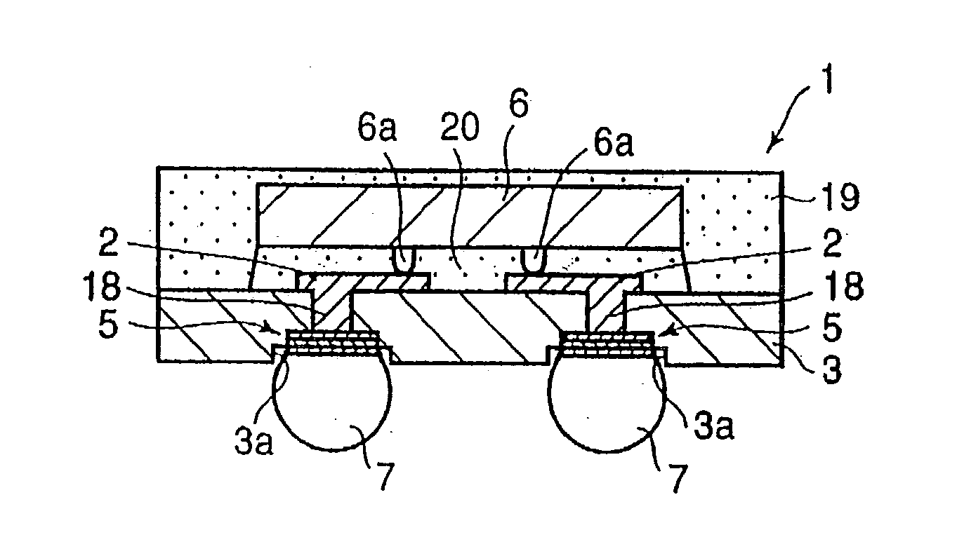
[0069] A method of fabricating semiconductor device 1 shown in FIGS. 4 and 6A through 6D according to the present invention will be described below with reference to FIGS. 9 and 10A through 13E.

[0070] Metal sheet 8 (see FIG. 8) for use as a matrix sheet for insulating layer 3 is prepared. For example, a metal sheet KFC (trade name, thickness 0.25 mm) manufactured by Kobe Steel, which is a copper sheet according to U.S. CDA standard C19210, is prepared. Metal sheet 8 is not limited to the material and thickness described above. Metal sheet 8 may be any metal sheet insofar as it is a good electric conductor for use as a cathode in a subsequent plating process, can be chemically dissolvable by an etchant, and can serve as a support plate for stacking insulating layer 3 and conductive layer 2 thereon. Metal sheet 8 may be a steel sheet, a nickel sheet, a stainless steel sheet, a sheet of an alloy of these metals, or a sheet plated with these metals, other than a copper sheet. The thickn...

2nd embodiment

[0088] A method of fabricating semiconductor device 1 according to a second embodiment will be described below with reference to FIGS. 10A through 10E, 11A through 11C, 14, 15A through 15F, and 16A through 16E. Those steps which are identical to those of the method according to the first embodiment will be described only briefly.

[0089] As with the first embodiment, the surface of copper sheet 8 shown in FIG. 10A is polished in step S1, and as shown in FIG. 10B, etching resists 9, 10 are laminated on respective opposite surfaces of copper sheet 8 in step S2. As shown in FIG. 10C, etching resist 9 on one surface of copper sheet 8 is patterned in step S3. Then, as shown in FIG. 10D, the areas of copper sheet 8 which are not covered with etching resist 9 are etched to a uniform depth in step S4. Then, as shown in FIG. 10E, photosensitive etching resists 9, 10 are removed.in step S5. Then, as shown in FIGS. 11A through 11DC, the entire surface of copper sheet 8 is etched again to remove ...

second embodiment

[0095] Then, a resin sheet with a copper foil, which has an insulating resin layer having a thickness ranging from 35 to 80 .mu.m and coated with an epoxy resin which is then partly cured, is placed on first insulating layer 21 and subjected to laminating press process. The copper foil is then removed by a copper etching process, forming second insulating layer 23 in step S24, as shown in FIG. 16A. In the second embodiment, therefore, two-layer insulating layer (interlayer insulating layer) 24 comprising first insulating layer 21 and second insulating layer 23 is constructed.

[0096] Then, as shown in FIG. 16B, via holes 23a are formed in second insulating layer 23, and epoxy resin scum is.removed therefrom by a desmearing process. Using copper sheet 8 as a cathode, an electric copper plating process is carried out to form a plated layer, which is patterned, producing vias 18 embedded in via holes 23a and conductive layer 2 serving as circuits in step S14, as shown in FIG. 16C.

[0097] ...


PUM

PropertyMeasurementUnit
Electrical conductoraaaaaaaaaa
aaaaaaaaaa

Abstract

To fabricate a semiconductor device, a pattern of recesses and lands is formed on a copper sheet as a matrix sheet, and BGA pads are formed on the lands on the copper sheet. An insulating layer is formed on the copper sheet to transfer the pattern of recesses and lands from the copper sheet to the insulating layer for thereby forming recesses in the insulating layer and placing BGA pads in the recesses in the insulating layer. Vias are formed through the insulating layer, and a conductive layer serving as circuits and interconnections is formed, the conductive layer being connected to the BGA pads by the vias. When the copper sheet is removed, the BGA pads are positioned within the recesses in the insulating layer. The BGA pads have surfaces positioned higher than the bottom of the recesses and lower than the surface of the insulating layer. A semiconductor chip is mounted on the conductive layer, and solder balls are joined to the BGA pads. Both the productivity of a process of mounting the solder balls and the bonding strength of the solder balls are increased.

Description

[0001] 1. Field of the Invention[0002] The present invention relates to a board for mounting a semiconductor chip thereon, a method of fabricating such a board, a semiconductor device, and a method of fabricating such a semiconductor device, and more particularly to a semiconductor device in a BGA (Ball Grid Array) type package, a multilayer wiring board for use in such a semiconductor device, and methods of fabricating such a semiconductor device and such a multilayer wiring board.[0003] 2. Description of the Related Art[0004] Heretofore, boards for mounting semiconductor chips thereon to make up BGA-type semiconductor devices comprise a glass epoxy multilayer wiring board or a build-up multilayer wiring board which is produced by stacking conductive layers and insulating layers repeatedly on a support plate of metal and then removing the support plate.[0005] The glass epoxy multilayer wiring board is made of an organic material having low heat resistance as a base material. Theref...

Claims


Application Information

Patent Timeline
IPC IPC(8): H01L23/12H01L21/48H01L21/56H01L21/68H01L23/13H01L23/31H01L23/498H05K1/11H05K3/20H05K3/46
CPCH01L21/4853Y10T29/49165H01L21/568H01L21/6835H01L23/13H01L23/3128H01L23/49816H01L23/49827H01L2221/68345H01L2224/16225H01L2224/73203H01L2224/73204H01L2924/01078H01L2924/01079H01L2924/15173H01L2924/15311H05K1/113H05K3/20H05K3/4614H05K2201/09036H05K2201/09472H01L2224/32225H01L21/563H01L2224/11334H01L2924/00
Inventor ITO, TOSHIHIDE
Owner NEC TOPPAN CIRCUIT SOLUTIONS
Features
  • Generate Ideas
  • Intellectual Property
  • Life Sciences
  • Materials
  • Tech Scout
  • Unparalleled Data Quality
  • Higher Quality Content
  • 60% Fewer Hallucinations
Learn More