Method of fabricating semiconductor device

a semiconductor device and manufacturing method technology, applied in the direction of polycrystalline material growth, crystal growth process, protective fluid, etc., can solve the problems of high temperature, increase in leakage current and breakdown voltage, and difficulty in applying deposition technology to the actual process of fabricating a semiconductor device at such high temperatures

Inactive Publication Date: 2003-08-28
NEC ELECTRONICS CORP
View PDF6 Cites 28 Cited by
  • Summary
  • Abstract
  • Description
  • Claims
  • Application Information

AI Technical Summary

Problems solved by technology

However, since the heat treatment at such high temperatures becomes a factor of thermal degradation of elements or wirings formed in the preceding processes it is difficult to apply a deposition technology at such high temperatures to an actual process of fabricating a semiconductor device.
Furthermore, as a deposition temperature becomes higher, grain sizes of the crystal constituting the ferroelectric film become larger, accordingly the irregularity of the film becomes larger, resulting in causing an increase in a leakage current and a decrease in the breakdown voltage.
Still furthermore, though it is not impossible to fabricate a ferroelectric film at temperatures as low as possible, atoms and ions diffuse insufficiently and poor crystallinity results, that is, it is difficult to obtain a high quality ferroelectric film.
Furthermore, unless the heat treatment is applied after the upper electrode is formed, owing to space charges and crystal defects formed in a boundary surface with the ferroelectric film at forming the upper electrode, inactive domains (a region where spontaneous polarization directions are aligned in the same direction) are contained, domains respond non-uniformly to an external electric field, and thereby lowering of the residual polarization or an increase in switching time may be caused.
In addition, unless the heat treatment after the formation of the upper electrode is not implemented, structural defects formed on a surface during the growth of the ferroelectric film or structural defects introduced on a surface o

Method used


Image

  • Method of fabricating semiconductor device
  • Method of fabricating semiconductor device
  • Method of fabricating semiconductor device

Examples


Embodiment Construction

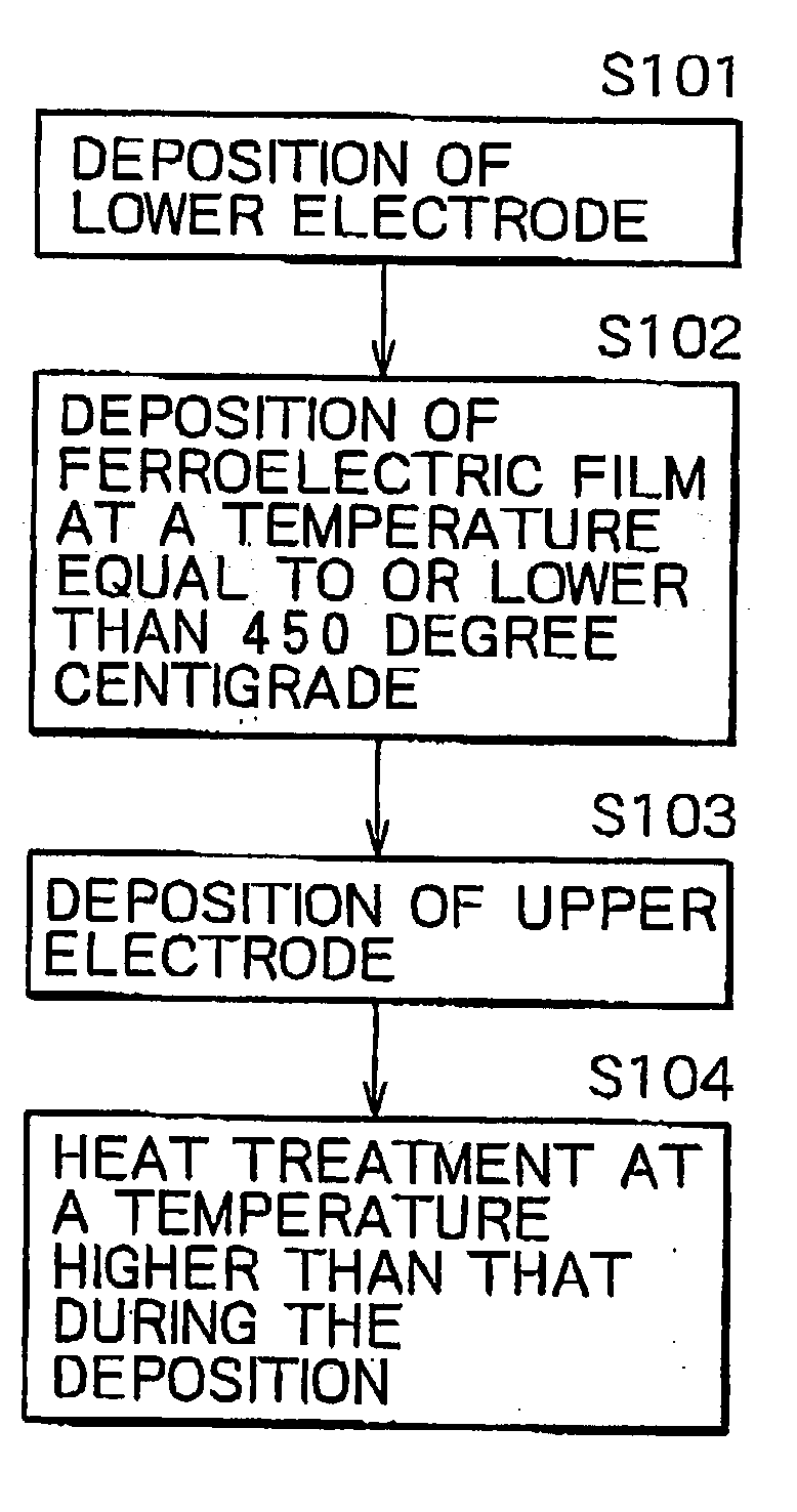
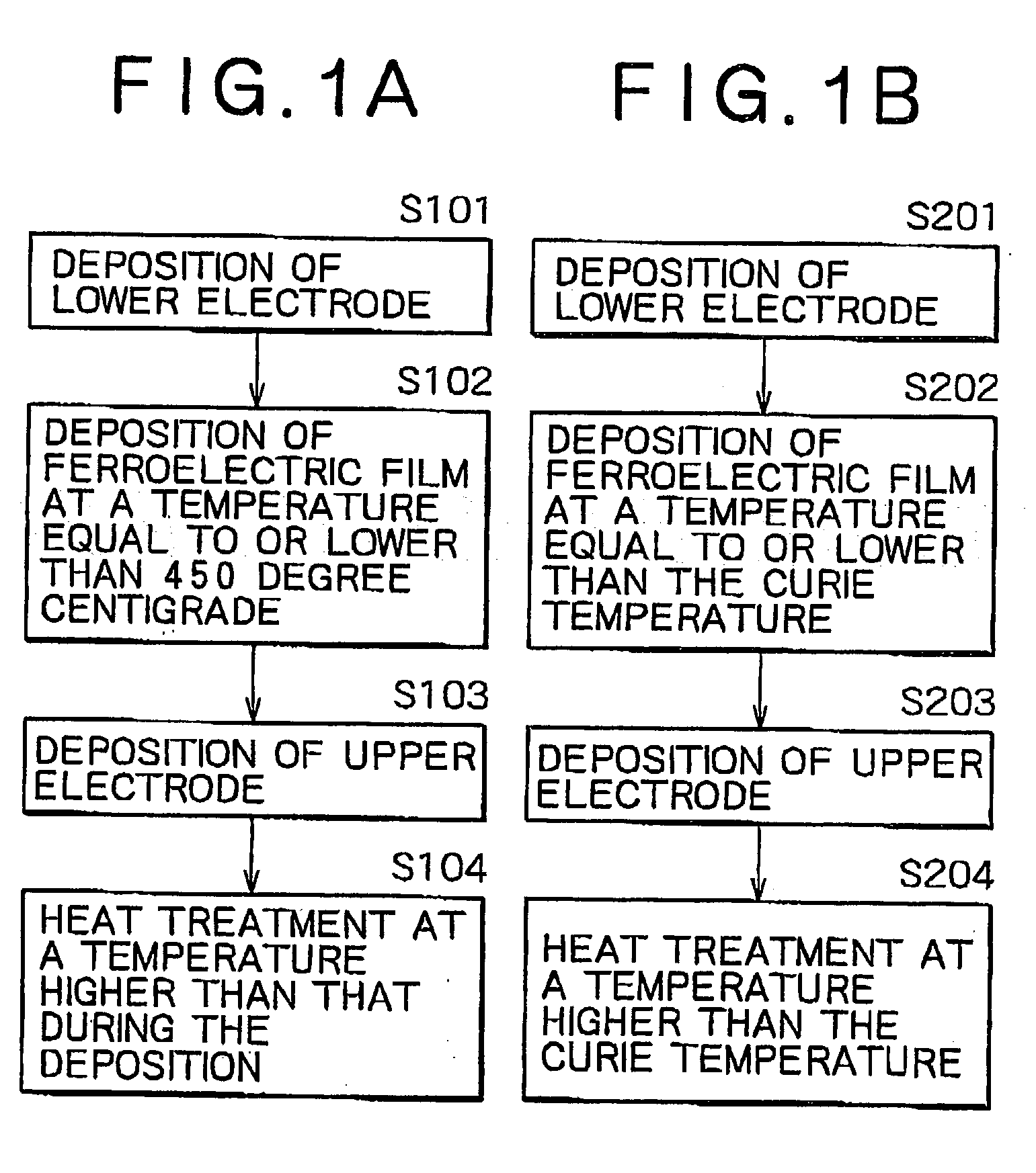
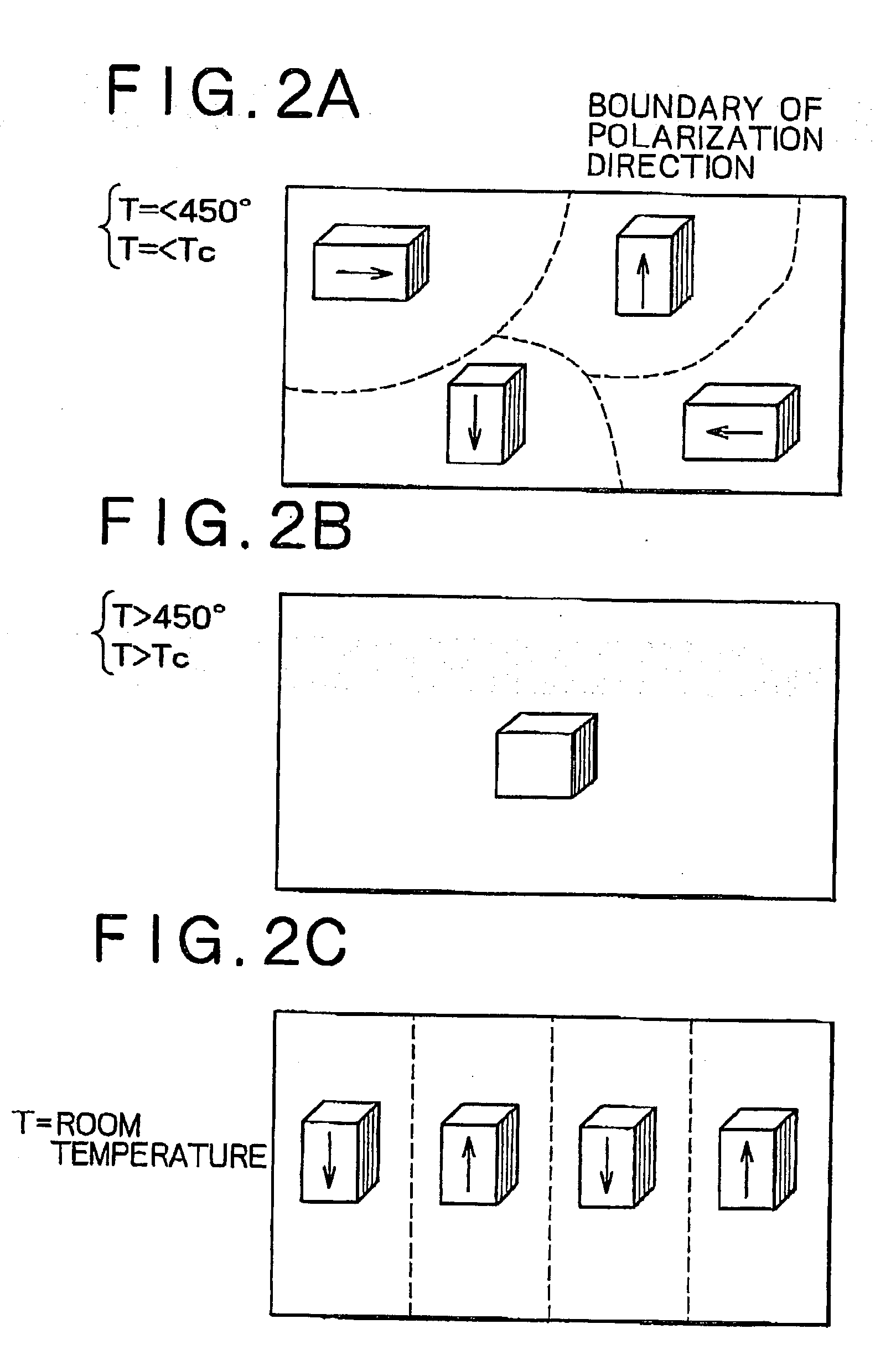
[0032] In the next place, an embodiment of the invention will be explained with reference to the drawings. The embodiment is an example in which the invention is applied to a so-called shadow RAM in which a ferroelectric capacitor is connected to an SRAM constituted of a MOS transistor. In the shadow RAM, as a circuit diagram thereof is shown in, for instance, FIG. 3, each of a pair of cascade connected N channel MOS transistors Q0, Q1 and a pair of cascade connected P channel MOS transistors Q2, Q3 is connected between a power supply VCC and a GND and both pairs are cross connected, to connection nodes N0, N1 thereof N channel MOS transistors Q4, Q5 are connected, respectively, and to these transistors a word line WL, bit lines BLN, BLT are connected. Furthermore, to the connection nodes N0, N1, ferroelectric capacitors F0, F1 are connected, and furthermore a plate line PL is connected thereto. Though detailed descriptions of the operation of the shadow RAM will be omitted, when po...


PUM

PropertyMeasurementUnit
Pressureaaaaaaaaaa
Angleaaaaaaaaaa
Angleaaaaaaaaaa

Abstract

On an insulating film on a surface of a substrate a lower electrode is formed, and on the lower electrode a ferroelectric film is formed at a temperature equal to or less than 450 degree centigrade, or at a temperature equal to or less than the Curie temperature of the ferroelectric film. Thereafter, on the ferroelectric film an upper electrode is formed, and after the upper electrode is formed, heat treatment is applied at a temperature higher than the deposition temperature or the Curie temperature. Thereby, a ferroelectric film having a particular crystal orientation is formed, and when heat treatment at a temperature higher than the deposition temperature or the Curie temperature is applied to transform once to a paraelectric phase, without altering a crystal structure, a ferroelectric phase can be obtained, and thereby a ferroelectric film aligned in the spontaneous polarization orientations of the respective domains can be obtained.

Description

[0001] 1. Technical Field of the Invention[0002] The present invention relates to a method of fabricating a semiconductor device, in particular to a method of fabricating a semiconductor device such as a semiconductor memory device provided with a capacitor having a ferroelectric film.[0003] 2. Description of the Related Art[0004] In recent semiconductor devices, in particular in semiconductor memory devices provided with transistors and capacitors, one that uses ferroelectric films for capacitor dielectrics has been proposed. So far, in a method of fabricating a capacitor provided with this kind of the ferroelectric films, after a lower electrode is formed on an insulating film on a surface of a semiconductor substrate, thereon a ferroelectric film is formed, further thereon an upper electrode is formed, and thereafter these upper electrode, ferroelectric film and lower electrode are formed into a predetermined pattern. Furthermore, in the fabricating method thereof, as a method of...

Claims


Application Information

Patent Timeline
IPC IPC(8): H01L21/02H01L21/314H01L21/316H01L21/8244H01L21/8246H01L27/105H01L27/11C23C16/40H01L27/115
CPCH01L21/02197H01L21/02271H01L21/02318H01L21/02356H01L21/3105H01L28/55H01L27/11H01L27/1104H01L27/11502H01L27/11507H01L21/31691H10B10/00H10B10/12H10B53/30H10B53/00H01L27/105
Inventor TAKEMURA, KOICHI
Owner NEC ELECTRONICS CORP
Why Eureka
Try Eureka