Method of polishing semiconductor wafers by using double-sided polisher

a technology of polishing machine and semiconductor wafer, which is applied in the direction of grinding machine, manufacturing tools, lapping machine, etc., can solve the problems of unstable rotation speed of silicon wafer within the holding hole of the corresponding wafer, inability to rotate well, and limited deference between said frictional resistances

Inactive Publication Date: 2003-09-25
SUMITOMO MITSUBISHI SILICON CORP
View PDF8 Cites 27 Cited by
  • Summary
  • Abstract
  • Description
  • Claims
  • Application Information

AI Technical Summary

Problems solved by technology

To fabricate a set of equipment for applying the double-sided polishing to those wafers of large gauge, such as 300 mm wafers, disadvantageously the carrier plate and thus the entire unit could be enlarged by a size to accommodate the sun gear.
However, there have been following problems in association with the method for double-sided polishing of the silicon wafers by using the double-sided polisher with no sun gear according to the prior art.
In specific, in the method of double-sided polishing of the wafer by the conventional apparatus, a direction of rotation as well as a speed of rotation of the silicon wafer within corresponding wafer holding hole has been unstable during polishing of the wafer.
This is because the frictional resistance acting on the front surface of t

Method used


Image

  • Method of polishing semiconductor wafers by using double-sided polisher
  • Method of polishing semiconductor wafers by using double-sided polisher
  • Method of polishing semiconductor wafers by using double-sided polisher

Examples


first embodiment

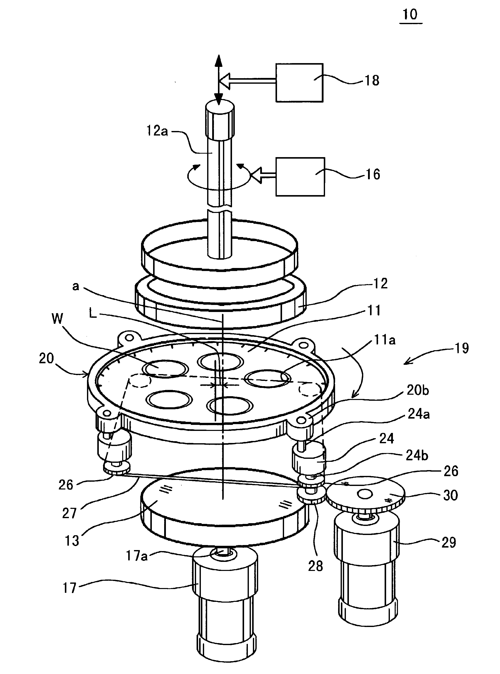
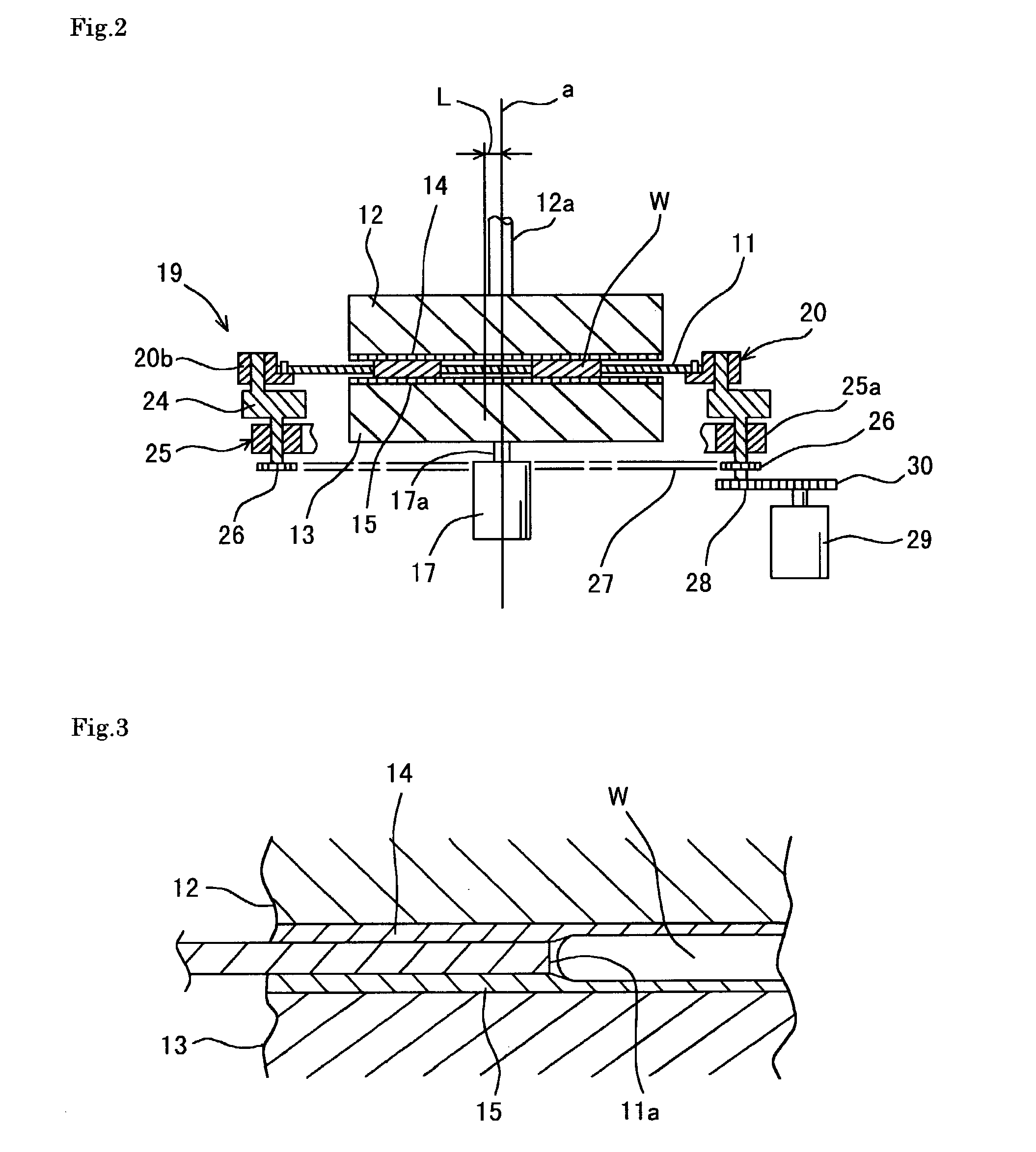
[0073] In FIG. 1 and FIG. 2, reference numeral 10 generally designates a double-sided polisher to which is applied a method of polishing the semiconductor wafer according to the present invention (hereafter, simply referred to as a double-sided polisher). This double-sided polisher 10 comprises a carrier plate 11 made of epoxy-glass having a circular disc-like shape in plan view in which five of wafer holding holes 11a have been formed by every 72 degrees (in the circumferential direction) around an axis line of the plate so as to penetrate through the plate, and a pair of upper surface plate 12 and lower surface plate 13 functioning for clamping silicon wafers "W", each having a diameter of 300 mm and having inserted and thus held operatively in the wafer holding hole 11a so as to be free to rotate therein, from above and below sides with respect to the wafers W and also functioning for polishing the surfaces of the wafers W by moving themselves relatively with respect to the silic...

second embodiment

[0100] Referring now to FIG. 9, a method of polishing semiconductor wafers by using a double-sided polisher according to the present invention will be described.

[0101] As shown in FIG. 9, this embodiment is representative of an example which has employed, instead of an upper surface plate 12 in the first embodiment, a surface plate 12A having a larger diameter than the lower surface plate 13.

[0102] This method also can create a difference between the frictional resistance acting on the front surface of the silicon wafer W from the upper surface plate 12A side and the frictional resistance acting on the back surface of the silicon wafer W from the lower surface plate 13 side in more positive manner as compared to the prior art. Consequently, the rotations of the silicon wafers W in respective wafer holding holes may be generated in a sure and steady manner.

[0103] Other description on configuration, operation and effect of this embodiment is almost same as in the first embodiment, whi...

third embodiment

[0104] Referring now to FIG. 10, a method of polishing semiconductor wafers by using a double-sided polisher according to the present invention will be described.

[0105] As shown in FIG. 10, this third embodiment is representative of an example which has employed, instead of the hard expanded urethane foam pad 14 having a circular shape in plan view extended over the upper surface plate 12 in the first embodiment, a hard expanded urethane foam pad 14A having a hexagonal shape in plan view.

[0106] In specific, since having a hexagonal shape, the polishing cloth 14 can create a difference in the frictional resistance in a positive manner with respect to the circular soft non-woven fabric pad on the lower surface plate 13. Consequently, during polishing of the wafers, the difference can be created more steadily as compared with the case of the prior art between the frictional resistance acting on the front surface of the wafer from the upper surface plate 12 side and the frictional resis...


PUM

PropertyMeasurementUnit
Lengthaaaaaaaaaa
Angular velocityaaaaaaaaaa
Timeaaaaaaaaaa

Abstract

An object of the present invention is to provide a method of polishing semiconductor wafer by using a double-sided polisher which prevents a polish-sagging in an outer periphery of the wafer and thereby improves a degree of flatness of the semiconductor wafer. During polishing of the semiconductor wafer by using a double-sided polisher, a larger difference as compared to the prior art is created between a frictional resistance acting on a front surface of a silicon wafer W from an upper surface plate 12 side and a frictional resistance acting on a back surface of the silicon wafer W from a lower surface plate 13 side. This is because the present invention has employed a hard expanded urethane foam pad 14 and a soft non-woven fabric pad 15, which have different friction coefficients to the silicon wafer W from each other. Thereby, respective wafers W can be rotated at such a high speed as 0.1-1.0 rpm within corresponding wafer holding holes 11a. Accordingly, the rotation of the wafer would not be suspended even if there were any defective condition induced during polishing. Further, partial variation or deviation in polishing volume particular in the outer periphery of the wafer would be hard to occur. Therefore, the polish-sagging is suppressed and thus the improved degree of flatness of the wafer W could be obtained. Further, during this polishing, the semiconductor wafer is polished in a state in which a part of the outer periphery of the semiconductor wafer is protruded by 3-15 mm beyond said respective polishing cloths. During polishing, the outer periphery of the wafer is polished while passing through its non-polishing region at each time when the semiconductor wafer is rotated by a predetermined angle. Therefore, a contact area per unit time of the outer periphery of the wafer with the polishing cloths is reduced as compared to the central region of the wafer. As a result, the polish-sagging in the outer periphery of the wafer is suppressed and the degree of flatness of the wafer is improved.

Description

[0001] The present invention relates to a method of polishing semiconductor wafers by using a double-sided polisher, and in more specific, to a method of polishing semiconductor wafers by using a double-sided polisher having no sun gear incorporated thereinto, thereby suppressing the polish-sagging thus to obtain the semiconductor wafers having highly improved flatness.DESCRIPTION OF THE PRIOR ART[0002] For manufacturing wafers having both surfaces polished according to the prior art, a single crystal silicon ingot is sliced to be formed into silicon wafers, and then those silicon wafers are subjected to a series of processing steps of beveling, lapping and acid etching in sequence. These steps are followed by a double-sided polishing process for mirror-finishing both front and back surfaces of the wafers. This double-sided polishing typically uses a double-sided polisher having an epicyclic gear system, in which a sun gear is disposed in the central region while an internal gear is...

Claims


Application Information

Patent Timeline
IPC IPC(8): B24B37/08B24B37/27B24B37/28H01L21/304
CPCB24B37/042B24B37/16B24B37/08H01L21/304
Inventor TANIGUCHI, TORUONO, ISOROKUHARADA, SEIJI
Owner SUMITOMO MITSUBISHI SILICON CORP
Why Eureka
Try Eureka