Semiconductor device and method of manufacturing the same

a semiconductor and semiconductor technology, applied in the direction of radiation control devices, transistors, electroluminescent light sources, etc., can solve the problems of inability to obtain crystals with aligned orientation, glass substrates with inferior heat resistance, and easy thermal deformation,

Inactive Publication Date: 2003-11-27
SEMICON ENERGY LAB CO LTD
View PDF59 Cites 127 Cited by
  • Summary
  • Abstract
  • Description
  • Claims
  • Application Information

AI Technical Summary

Problems solved by technology

A glass substrate is inferior in heat resistance and is easily subjected to thermal deformation.
As a result, continuous wave oscillation lasers are now suddenly attracting attention.
However, when a laser light is irradiated to an amorphous semiconductor film formed over a flat surface for crystallization, crystals become polycrystals, thereby arbitrarily forming defects such as a grain boundaries, so that crystals with aligned orientation cannot be obtained.
The position and size of the crystal grains are random, and it is difficult to specify the crystal grain position and size when forming a crystalline semiconductor film.
Therefore the crystallinity of a channel formation region of the TFT cannot be controlled strictly.
The randomly-formed grain boundaries and crystal defects degrade the characteristics and cause fluctuation in characteristics between elements.
However, it is nearly impossible to form an amorphous silicon film, in which grain boundaries do not exist, by using a laser annealing method.
It has therefore not been possible to date to obtain characteristics equivalent to those of a MOS transistor, which is manufactured on a single crystal silicon substrate, in a TFT that uses a crystalline silicon film crystallized by employing laser annealing.
However, a single cr

Method used


Image

  • Semiconductor device and method of manufacturing the same
  • Semiconductor device and method of manufacturing the same
  • Semiconductor device and method of manufacturing the same

Examples


embodiment mode 9

[0257] Embodiment Mode 9

[0258] The present invention can be used in various devices. Examples thereof include portable information terminals (electronic schedulers, mobile computers, cellular phones, and the like), video cameras, digital cameras, personal computers, television monitors, projection display devices, etc. FIGS. 28A to 29D show examples of the devices.

[0259] FIG. 28A shows an example of applying the present invention to a television monitor. The device is composed of a case 3001, a supporting base 3002, a display unit 3003, and others. A TFT manufactured in accordance with the present invention can be used in the display unit 3003 and, in addition, various integrated circuits formed on a glass substrate, such as various logic circuits, high-frequency circuits, memories, microprocessors, media processors, and graphics LSIs.

[0260] FIG. 28B shows an example of applying the present invention to a video camera. The device is composed of a main body 3011, a display unit 3012,...

embodiment 1

[0279] Embodiment 1

[0280] This embodiment shows an example of manufacturing a TFT in which a crystalline semiconductor film is formed on a base insulating film having an opening, and a channel formation region is disposed in a filled region filling the opening.

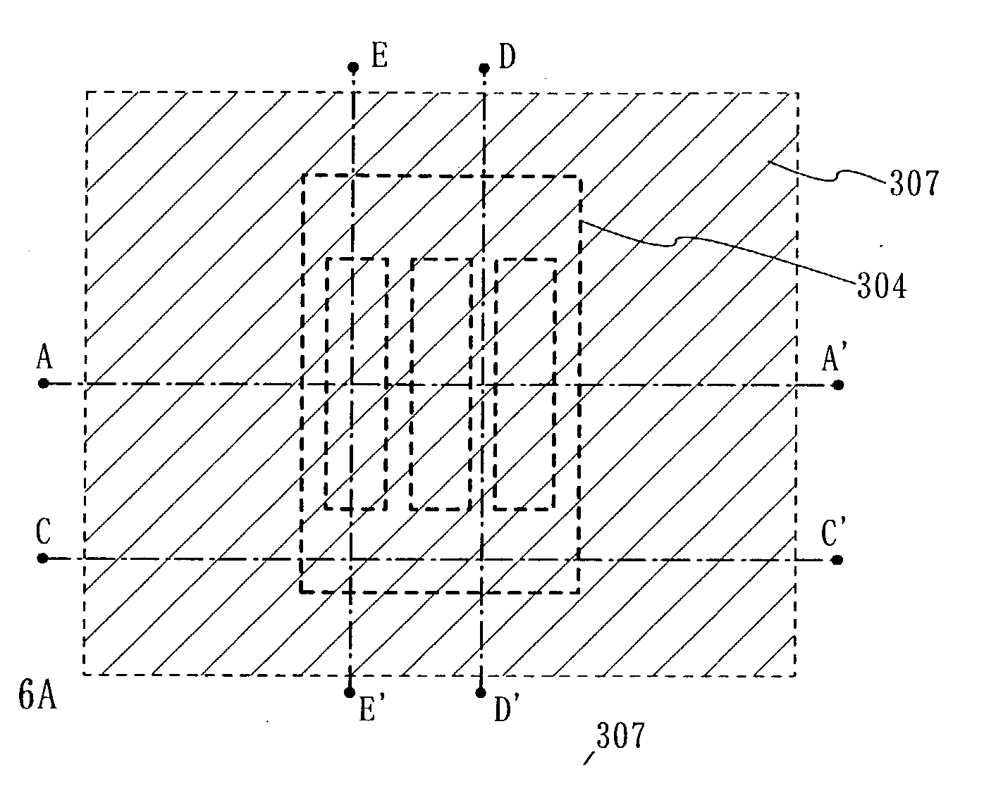
[0281] A first insulating film 5602 is formed by a 100 nm silicon oxynitride film on a glass substrate 5601 in FIGS. 36A to 36C. A silicon oxide film is formed on the first insulating film 5602, and second insulating films 5603 having a rectangular shape pattern are formed by photoetching. The silicon oxide film is deposited to a thickness of 150 nm by using plasma CVD with a mixture of TEOS and O.sub.2, and by discharging at a high frequency (13.56 MHz) electric power density of 0.6 W / cm.sup.2 with a reaction pressure of 40 Pa and a substrate temperature of 400.degree. C. Openings 5604a and 5604b are then formed by etching.

[0282] Note that FIG. 36A is an upper surface diagram, FIG. 36B is a longitudinal cross sectional diagra...

embodiment 2

[0289] Embodiment 2

[0290] Embodiment 2 shows a structure formed by processes that are similar to those of Embodiment 1, but as shown by FIGS. 41A to 41C, the openings formed in the second insulating films 5603 are formed in long, thin strip regions and regions that are connected to the long, thin strip regions. As island-like semiconductor region 5620 is formed by a crystalline silicon film in alignment with the opening 5604c, and a multi-channel TFT can be completed by forming a gate insulating film 5621 and a gate electrode 5622.


PUM


Abstract

An objective is to provide a method of manufacturing a semiconductor device, and a semiconductor device manufactured by using the manufacturing method, in which a laser crystallization method is used that is capable of preventing the formation of grain boundaries in TFT channel formation regions, and is capable of preventing conspicuous drops in TFT mobility, reduction in the ON current, and increases in the OFF current, all due to grain boundaries. Stripe shape or rectangular shape unevenness or opening is formed. Continuous wave laser light is then irradiated to a semiconductor film formed on an insulating film. Note that although it is most preferable to use continuous wave laser light at this point, pulse wave oscillation laser light may also be used.

Description

[0001] 1. Field of the Invention[0002] The present invention relates to a semiconductor device formed by using a semiconductor film having a crystalline structure (crystalline semiconductor film), and to a method of manufacturing the semiconductor device. The present invention particularly relates to a semiconductor device containing a field effect transistor in which a channel formation region is formed by a crystalline semiconductor film formed on an insulating surface, and to a method of manufacturing the semiconductor device.[0003] 2. Description of the Related Art[0004] In recent years, a technique of forming a thin film transistor (TFT) over a substrate has greatly progressed, and its application and development for active matrix semiconductor display devices have been advanced. A thin film transistor (hereinafter referred to as TFT) which is manufactured by using a semiconductor film having a crystalline structure has been applied to flat panel displays represented by a liqui...

Claims


Application Information

Patent Timeline
IPC IPC(8): H01L21/336H01L21/77H01L21/84H01L27/12H01L27/148H01L29/04H01L29/786H05B44/00
CPCH01L27/12H01L27/148H01L29/04H01L29/66757H01L27/1281H01L29/78621H01L29/78675H01L29/78696H01L29/785
Inventor ISOBE, ATSUOYAMAZAKI, SHUNPEIKOKUBO, CHIHOTANAKA, KOICHIROSHIMOMURA, AKIHISAARAO, TATSUYAMIYAIRI, HIDEKAZUAKIBA, MAI
Owner SEMICON ENERGY LAB CO LTD
Why Eureka
Try Eureka