Substrate treating method, substrate-processing apparatus, developing method, method of manufacturing a semiconductor device, and method of cleaning a developing solution nozzle

Inactive Publication Date: 2004-02-12
KK TOSHIBA
View PDF6 Cites 27 Cited by
  • Summary
  • Abstract
  • Description
  • Claims
  • Application Information

AI Technical Summary

Problems solved by technology

When so-called impurities and contaminants are left in this manner, in a process of using the pattern of the photo resist as a mask to subject the film to be processed (e.g., the insulating film, conductive film forming a material of a wiring layer) to etching processing, an error of dimension is generated, and yield drops in the manufacturing of the semiconductor device.
When the bore diameter of the semiconductor substrate is enlarged, that is, when an area of the substrate increases, many problems are generated in using the related-art cleaning method.
However, the peripheral edge of the semiconductor substrate is not directly hit by the cleaning solution with a sufficient pressure, and is low in the cleaning effect as compared with the middle portion of the semiconductor substrate and the vicinity of the portion.
Therefore, with the enlargement of the bore diameter of the substrate, a physical load is further added, and the pattern of the photo resist formed by the developing treatment is adversely influenced.
A phenomenon remarkably occurs in which the pattern of the photo resist formed by the developing treatment is damaged or pattern falling is generated.
With the miniaturization of the dimension of the semiconductor device, the developing solution does not su

Method used


Image

  • Substrate treating method, substrate-processing apparatus, developing method, method of manufacturing a semiconductor device, and method of cleaning a developing solution nozzle
  • Substrate treating method, substrate-processing apparatus, developing method, method of manufacturing a semiconductor device, and method of cleaning a developing solution nozzle
  • Substrate treating method, substrate-processing apparatus, developing method, method of manufacturing a semiconductor device, and method of cleaning a developing solution nozzle

Examples


second embodiment

[0120] In the present embodiment, the developing, cleaning, and drying treatments are performed in order to form the pattern which has a predetermined dimension and shape in the region to be treated of the substrate in the same manner as in the first embodiment. Moreover, in the present embodiment, a so-called developing treatment apparatus of a single wafer process system is used in which one substrate can continuously be subjected to the process of the developing, cleaning, and drying treatments in one apparatus.

[0121] A treatment unit which can continuously perform the developing, cleaning, and drying treatments with respect to the substrate is disposed in the developing treatment apparatus. In the present embodiment, each corresponding treating mechanism is used to perform a series of processes of the developing, cleaning, and drying treatments in this treating unit.

[0122] As one example, the developing treatment mechanism is disposed to perform the known scan developing treatme...

third embodiment

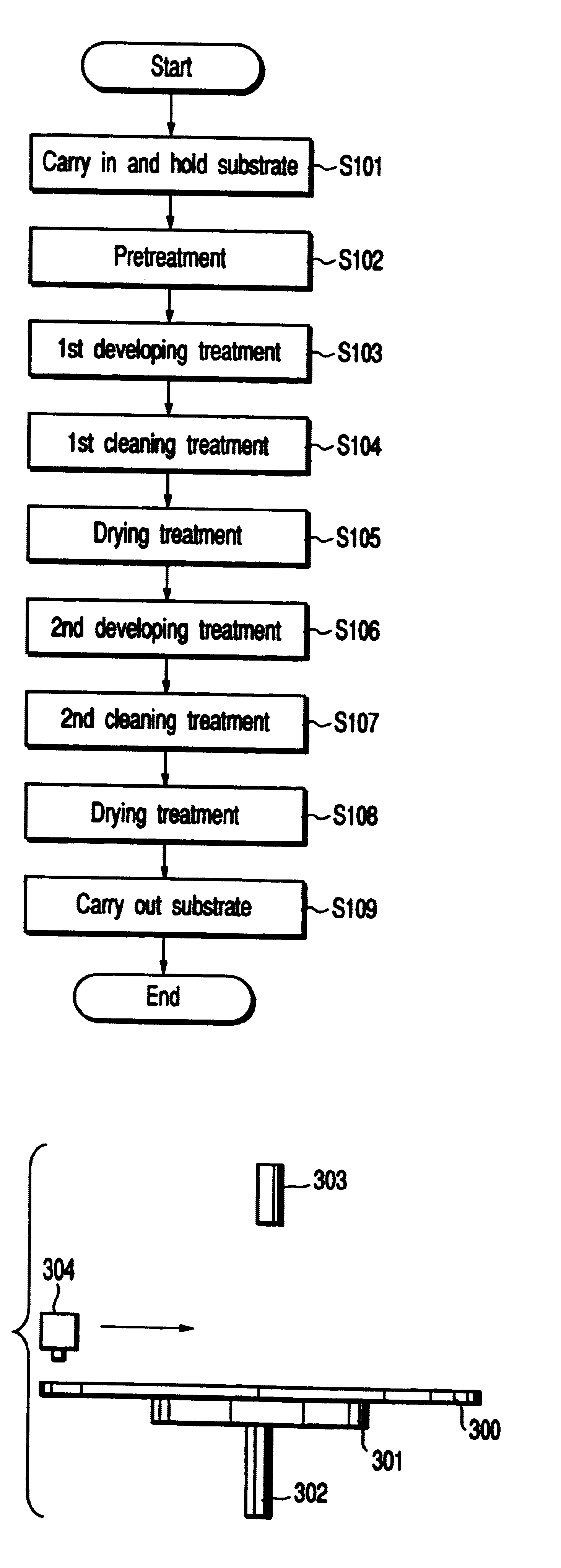
[0198] FIG. 11 is a diagram showing a flowchart of a treating procedure of the developing treatment method according to a third embodiment of the present invention. Moreover, FIGS. 12 to 16 are process diagrams showing the treating procedure of the developing treatment method according to the third embodiment of the present invention.

[0199] A developing method according to the third embodiment of the present invention will be described with reference to FIGS. 11 to 16.

[0200] (Step S101)

[0201] As shown in FIG. 12, a main surface of a substrate 300 including the semiconductor substrate is coated with the resist of the chemical amplification type (photosensitive resist film) via the reflection preventive film, and KrF excimer laser is used in the chemical amplification type resist film to reduce / project / expose a circuit pattern via a reticle for exposure. The substrate 300 is subjected to PEB treatment. Subsequently, a transfer robot transfers the substrate 300 into an upper part of a ...

fourth embodiment

[0250] FIG. 19 is a diagram showing a flowchart of the development treating procedure according to a fourth embodiment of the present invention.

[0251] Since steps S201 to S203 are similar to the steps S101 to S103 described in the third embodiment, the description thereof is omitted.

[0252] (Steps S204, S205)

[0253] The low-concentration ozone water was discharged from the rinse nozzle in about five seconds after the developing solution film was formed in the substrate main surface in step S203. Subsequently, the substrate was rotated, and almost all the cleaning solution was removed, but without drying the substrate, the cleaning solution was slightly left, and the ozone water film was formed.

[0254] (Step S206)

[0255] Subsequently, the developing solution for processing the resist film on the substrate was formed on the substrate in which the ozone water film was formed. The forming method of the developing solution film is similar to that of the third embodiment.

[0256] Since steps S2...


PUM

PropertyMeasurementUnit
Fractionaaaaaaaaaa
Lengthaaaaaaaaaa
Timeaaaaaaaaaa

Abstract

There is disclosed a substrate treating method comprising supplying a treating solution onto a substrate, and continuously discharging a first cleaning solution to the substrate from a first discharge region disposed in a nozzle, while moving the nozzle and substrate with respect to each other in one direction, wherein a length of a direction crossing at right angles to the direction of the first discharge region is equal to or more than a maximum diameter or longest side of the substrate, the nozzle continuously spouts a first gas to the substrate from a first jet region, and the length of a direction crossing at right angles to the direction of the first jet region is equal to or more than the maximum diameter or longest side of the substrate.

Description

[0001] This application is based upon and claims the benefit of priority from the prior Japanese Patent Applications No. 2002-17937, filed Jan. 28, 2002, and No. 2002-57764, filed Mar. 4, 2002, the entire contents of which are incorporated herein by reference.[0002] 1. Field of the Invention[0003] The present invention relates to a substrate treating method and substrate treating apparatus in which a treating solution is used to treat a substrate and which are particularly for use in performing a cleaning treatment subsequently to a developing treatment in a process of manufacturing a semiconductor device.[0004] 2. Description of the Related Art[0005] When a semiconductor device, liquid crystal display device, and electronic circuit component are manufactured, a substrate is subjected to a developing treatment and thereafter successively subjected to cleaning and drying treatments so as to form a pattern in a process of forming a circuit including a device, wiring, and the like.[000...

Claims


Application Information

Patent Timeline
IPC IPC(8): G03F7/30H01L21/311H01L21/027
CPCG03F7/3021Y10S134/902H01L21/31133G03F7/3057H01L21/6704
Inventor HAYASAKI, KEIITO, SHINICHIEMA, TATSUHIKOTAKAHASHI, RIICHIRO
Owner KK TOSHIBA
Why Eureka
Try Eureka