Supercharge Your Innovation With Domain-Expert AI Agents!

Semiconductor storage device and controlling method therefor

a technology of magnetic storage and storage device, which is applied in the direction of digital transmission, generating/distributing signals, instruments, etc., can solve the problem of more time-consuming read operation than write operation

Active Publication Date: 2004-02-19
RENESAS ELECTRONICS CORP
View PDF3 Cites 11 Cited by
  • Summary
  • Abstract
  • Description
  • Claims
  • Application Information

AI Technical Summary

Benefits of technology

The present invention provides a semiconductor storage device that improves operating frequency by alternating read and write cycles. The device includes a first circuit activated for a predetermined preset time based on a first transition of a clock signal, a second circuit activated for a predetermined preset time based on a second transition of the clock signal, and a circuit for controlling the timing of the second circuit to overlap with the first circuit. The device also includes an address register for sampling an input address signal, a read pulse generating circuit for generating a read pulse signal, a write pulse generating circuit for generating a write pulse signal, and a memory cell array with a plurality of memory cells. The device can operate faster and more efficiently by alternating read and write cycles.

Problems solved by technology

Thus, in a cell array block, the read operation is more time-consuming than the write operation.

Method used


Image

  • Semiconductor storage device and controlling method therefor
  • Semiconductor storage device and controlling method therefor
  • Semiconductor storage device and controlling method therefor

Examples


Embodiment Construction

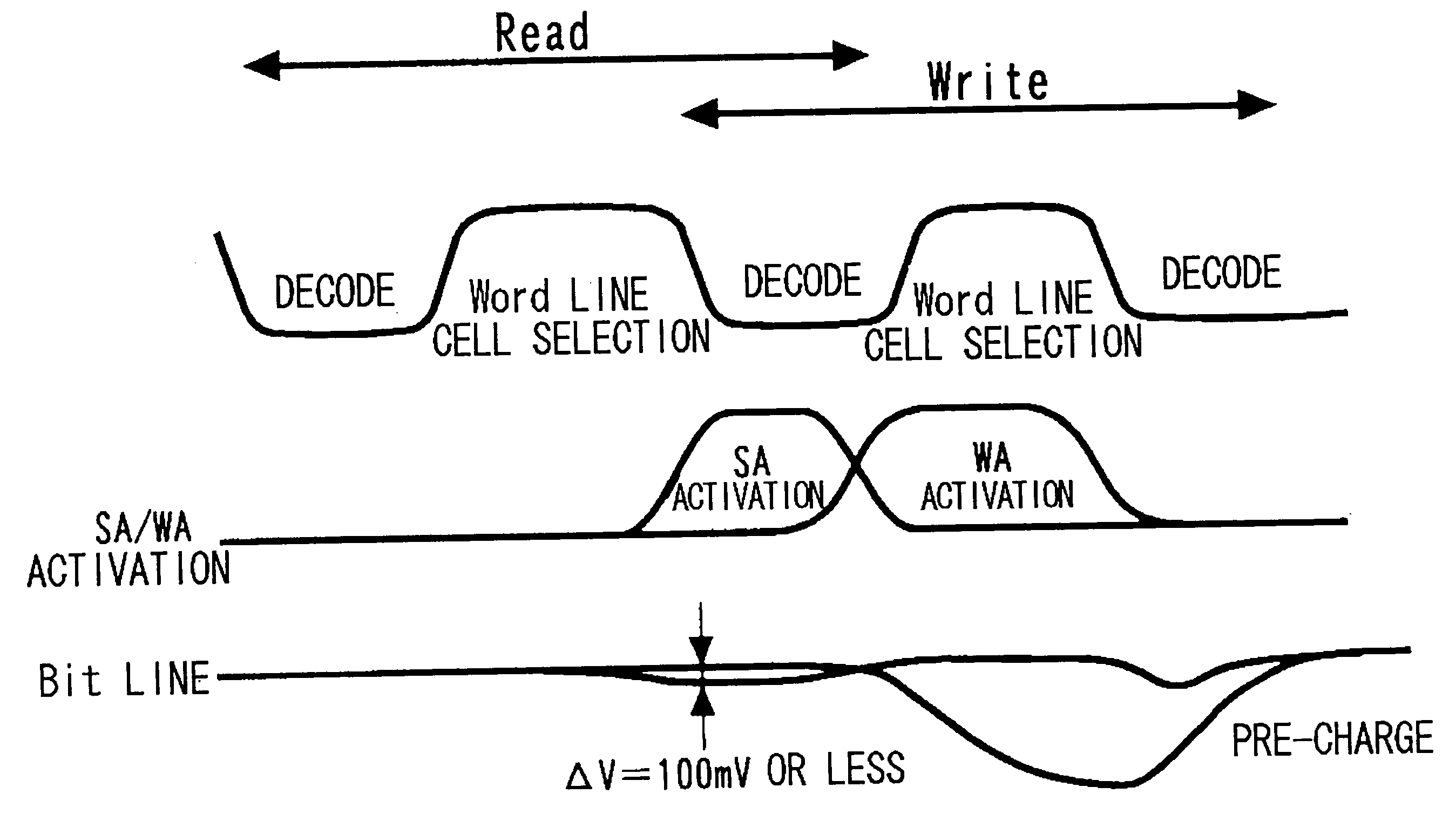
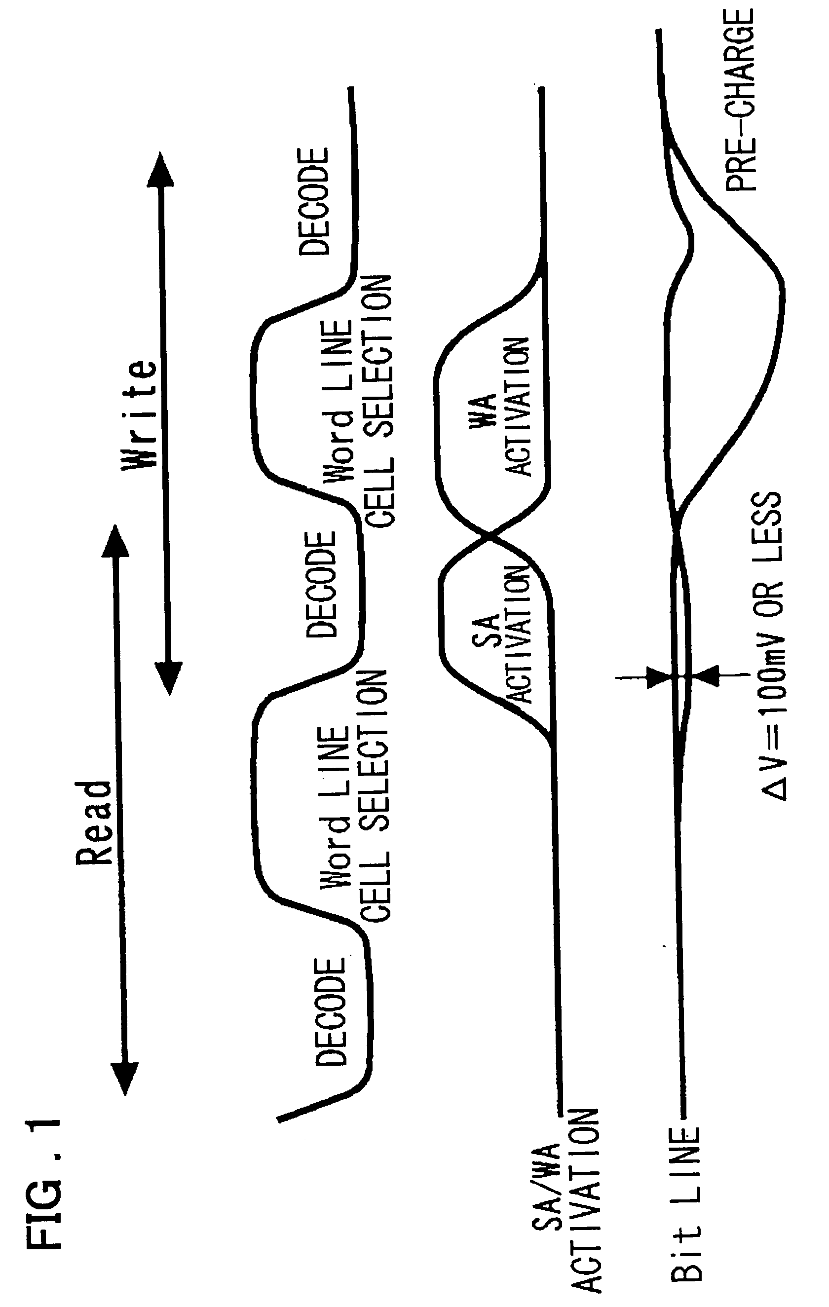
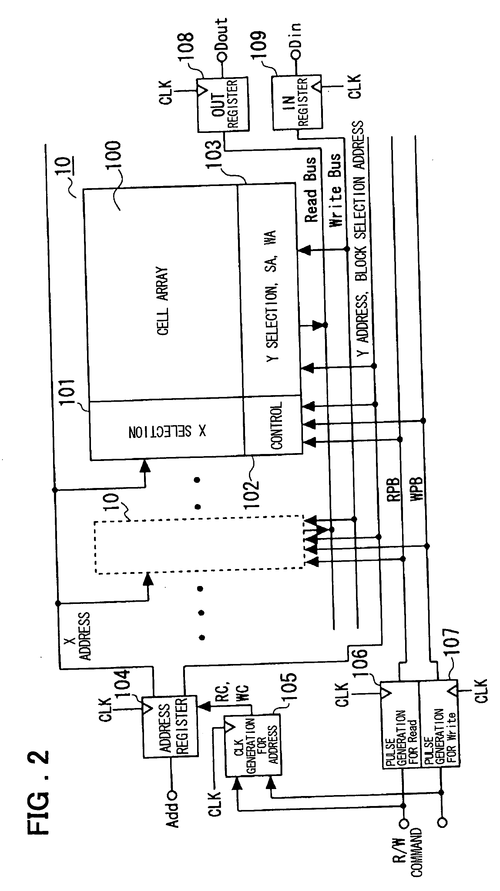
[0051] Several embodiments of the present invention are hereinafter explained. A semiconductor device, according to one embodiment of the present invention, comprises first to sixth circuits as described below. The first circuit (e.g. an address decoder circuit, such as an address register, an X-selection circuit or a Y-selection circuit) is activated for a predetermined preset period when one of a first control signal generated based on a first transition of an input clock signal and a second control signal generated based on a second transition of a cycle next following the first transition of the clock signal is activated. The second circuit (such as a word line driving circuit for selecting a word line in the X-selection circuit of FIG. 2, and a control circuit therefor, see FIG. 5C) is activated for a predetermined preset period when one of a third signal generated based on the first transition of the clock signal and a fourth signal generated based on a second transition of a ...


PUM


Abstract

A semiconductor storage device includes a circuit receiving a command signal for generating a read control signal (RPB) based on the transition of a clock signal CLK and a circuit receiving the command signal for generating a write control signal (WPB) based on the transition of the clock signal CLK. The read cycle in which decoding of an address, selection of a word line and activation of a sense amplifier are executed based on the read control signal to read cell data, and the write cycle in which decoding of an address, selection of a word line and activation of a write amplifier are executed based on the write control signal and bit line pre-charging is also carried out, are carried out alternately. The sense period of the read cycle is overlapped with the decoding period of the write cycle.

Description

[0001] This invention relates to a semiconductor storage device and, more particularly, to an architecture of a semiconductor storage device suited for improving operating speed and method for controlling the semiconductor storage device.[0002] Recently, an ultra-high-speed optical communication standard, such as OC-192 (10 Gbps) or OC-768 (40 Gbps) has obtained general acceptance in communication equipment, such as a switch or a router. As an SRAM (static random access memory) technique for implementing the data transfer rate complying with these standards, QDR (Quad Data Rate) / DDR (Double Data Rate) has been jointly developed. For example, QDRII / DDRII SRAM is of the specifications supporting the maximum operating frequency up to 333 MHz (NEC Press Release: Apr. 15, 2002-2: "http: / / www.nec.co.jo / press / ja / 0204 / 1502 / html"). In the QDRII architecture, a data port is divided into an input port and an output port (I / O separation), these ports each operating at a double rate. Meanwhile, ...

Claims


Application Information

Patent Timeline
Patent Type & Authority Applications(United States)
IPC IPC(8): G11C11/413G11C11/407G11C11/41G11C11/417G11C11/419
CPCG11C11/419G11C11/41
Inventor TAKAHASHI, HIROYUKIMATSUI, YUUJISONODA, MASATOSHIKATO, YOSIYUKI
Owner RENESAS ELECTRONICS CORP
Features
  • R&D
  • Intellectual Property
  • Life Sciences
  • Materials
  • Tech Scout
  • Unparalleled Data Quality
  • Higher Quality Content
  • 60% Fewer Hallucinations
Learn More