DFB semiconductor laser device having ununiform arrangement of a diffraction grating

a semiconductor laser and diffraction grating technology, applied in the direction of laser details, laser optical resonator construction, optical resonator shape and construction, etc., can solve the problem of difficult in fact to achieve such a low coupling factor, excessively high .kappa value impairing high output power, etc. problem

Active Publication Date: 2004-03-04
FURUKAWA ELECTRIC CO LTD
View PDF10 Cites 22 Cited by
  • Summary
  • Abstract
  • Description
  • Claims
  • Application Information

AI Technical Summary

Problems solved by technology

More specifically, an excessively higher .kappa. value impairs a high output power, whereas an extremely lower .kappa. value prevents the single-mode emission.
It is difficult in fact to achieve such a low coupling factor, however.
The mentioned smaller thickness or the smaller difference requires a higher accuracy in the fabrication process of the laser device, and is generally difficult to employ in the mass production of the laser devices.
Thus, it is difficult to fabricate DFB laser devices having excellent single-mode characteristic in the conventional technique with a higher product yield.
However, this structure causes a discontinuity of the electric field at the boundary between the area including the diffraction grating and the area including no diffraction grating, raising the problem of ununiformity of the carrier density in the injected current.
Thus, the gain difference between the lasing modes may be reduced, which causes an inter-mode transition in the laser device at a higher output power range, thereby generating an undesirable kink in the current dependency characteristic of the optical output power.
In the meantime, a conventional DFB laser device having a low-reflection coating film formed at the front facet of the laser cavity and a high-reflection coating film formed at the rear facet, as described before, generally involves a problem of hole burning, which causes an increase of the spectral linewidth in the laser emission.

Method used


Image

  • DFB semiconductor laser device having ununiform arrangement of a diffraction grating
  • DFB semiconductor laser device having ununiform arrangement of a diffraction grating
  • DFB semiconductor laser device having ununiform arrangement of a diffraction grating

Examples


first embodiment

[0040] First Embodiment

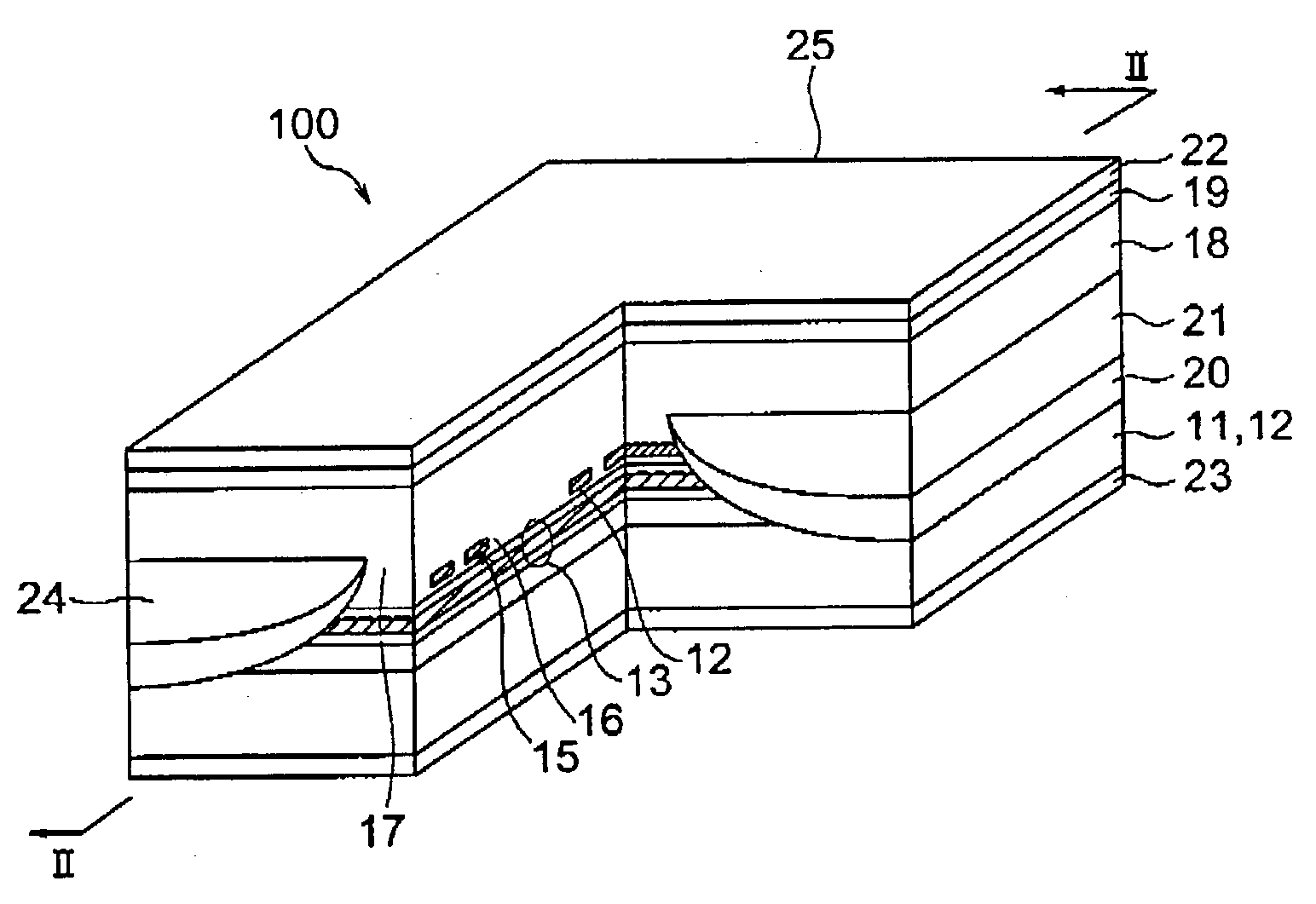
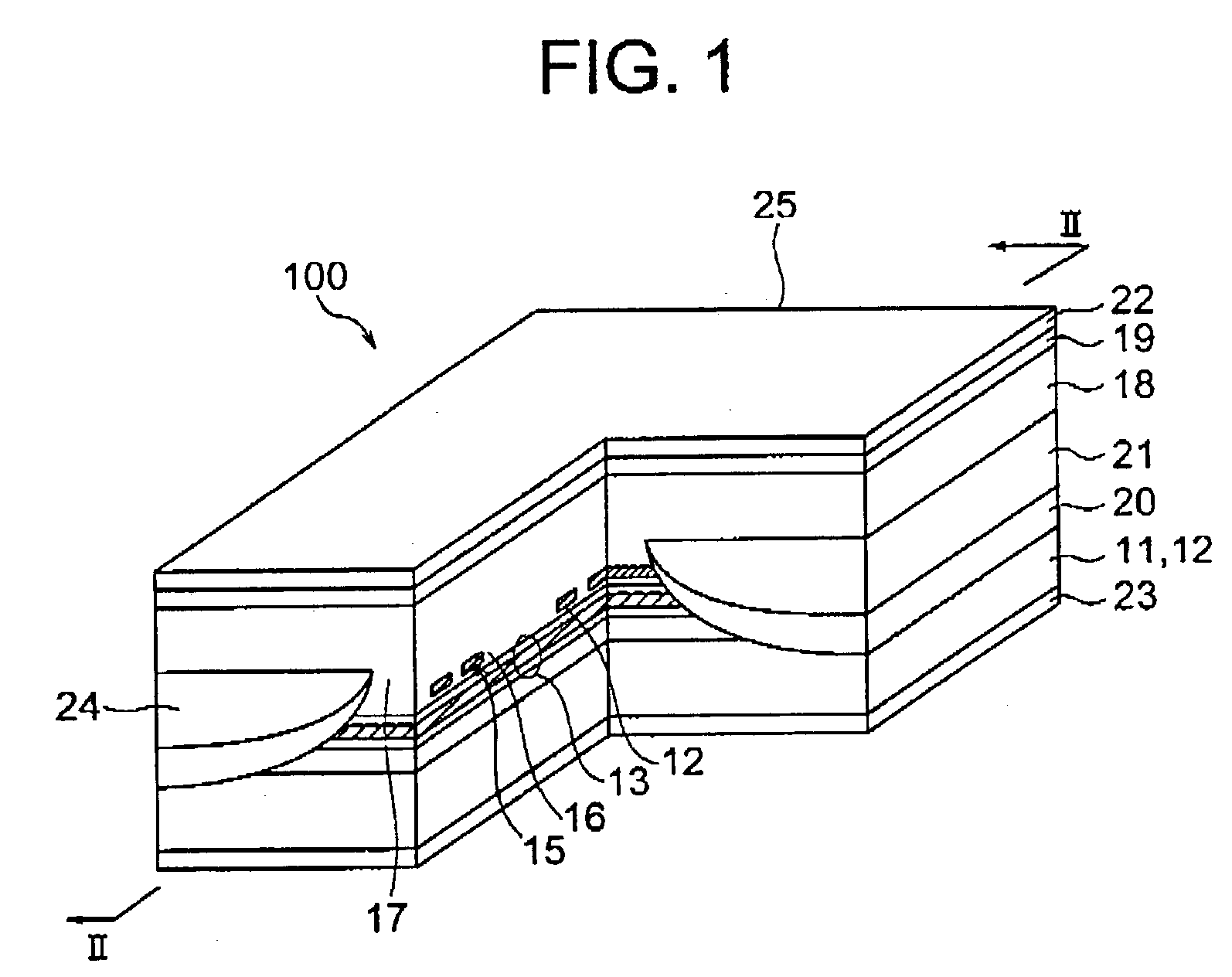
[0041] Referring to FIG. 1, a DFB laser device, generally designated by numeral 100, according to a first embodiment of the present invention is configured as a buried-heterostructure DFB laser device having a cavity length of 1200 .mu.m and an emission wavelength of 1550 nm. The DFB laser device 100 includes an n-InP substrate 11 having a thickness of about 120 .mu.m, and a layer structure including n-InP buffer layer 12, active layer 13 of a multiple-quantum-well separate confinement heterostructure (MQW-SCH), p-InP spacer layer 14, 10-nm-thick diffraction grating 15, p-InP buried layer 16 buried the diffraction grating 15, and p-InP cladding layer 17, which are consecutively formed on the n-InP substrate 11. The MQW-SCH active layer 13 includes therein six quantum well layers in this example.

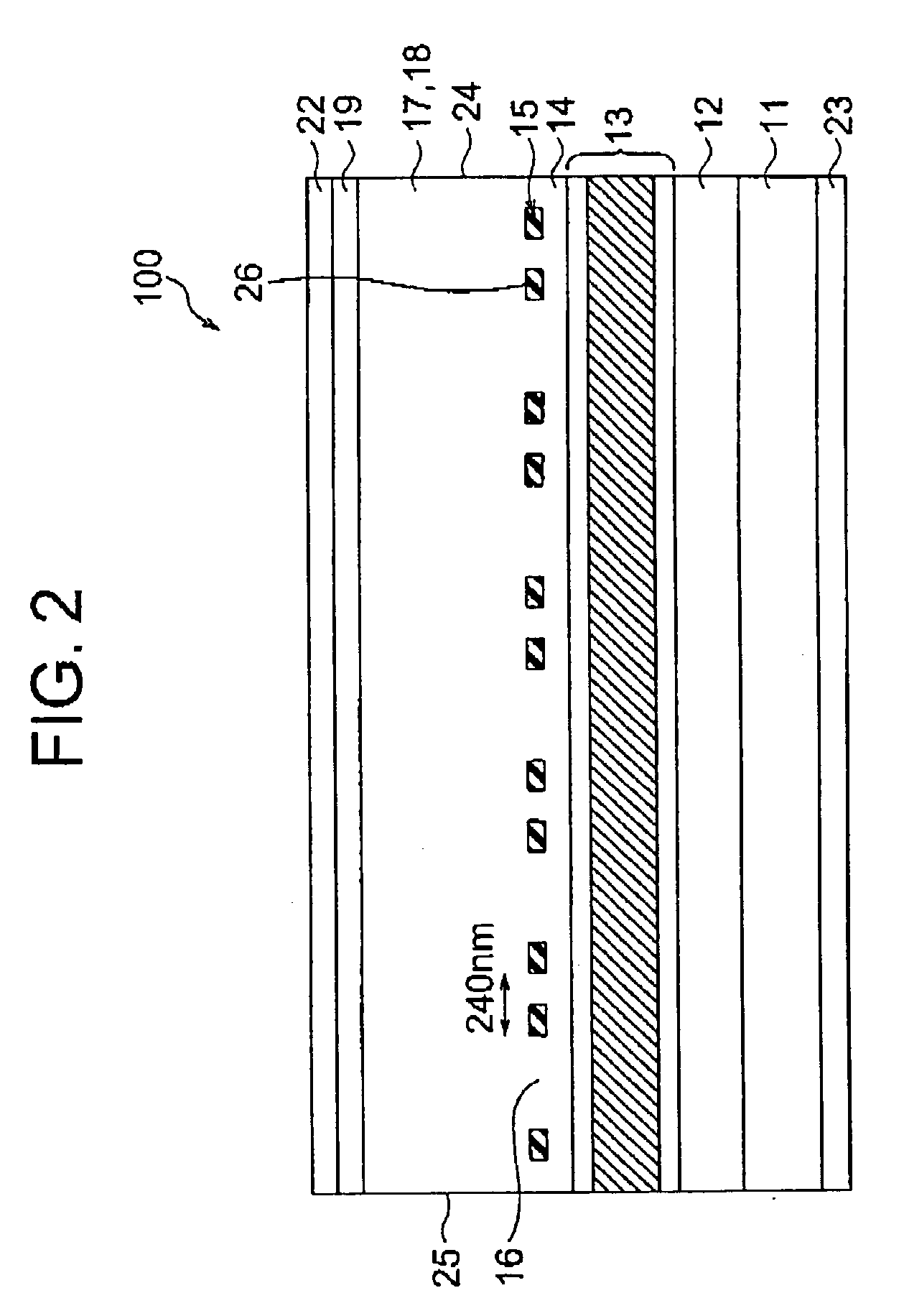
[0042] The diffraction grating 15 is made of quaternary semiconductor, InGaAsP, having a bandgap wavelength .mu.g of 1100 nm. Referring to FIG. 2, the diffraction grati...

second embodiment

[0061] Second Embodiment

[0062] Referring to FIGS. 5A to 5D, there are shown schematic top plan views of the diffraction gratings of DFB laser devices of first to fourth examples according to a second embodiment of the present invention In FIG. 5A, the DFB laser device of the first example of the present embodiment has a partial diffraction grating structure which includes a pair of diffraction grating areas 29 each having therein a diffraction grating and a pair of Fabry-Perot areas 30 each having therein no diffraction grating, which are alternately arranged from the rear facet 25 to the emission facet (front facet) 24 of the laser cavity along the axial direction thereof. The diffraction grating of the diffraction grating area 29 is similar to the diffraction grating shown in FIG. 2 except that the diffraction grating of the diffraction grating area 29 has a uniform arrangement of the corrugation patterns.

[0063] The ratio of the length of the diffraction grating area 29 to the len...

third embodiment

[0071] Third Embodiment

[0072] Referring to FIG. 8, a DFB laser device, generally designated by numeral 101, according to a third embodiment of the present invention has an emission wavelength of 1550 nm, a cavity length of 500 .mu.m, and a specific structure for the diffraction grating, which provides a larger value for the coupling factor .kappa. in the vicinity of the front facet of the laser cavity and a smaller value for the vicinity of the rear facet of the laser cavity.

[0073] More specifically, the DFB laser device 101 of the present embodiment includes a 120-.mu.m-thick n-InP substrate 11, and a layer structure including n-InP buffer layer 12, MQW-SCH active layer 13, p-InP spacer layer 14, InGaAsP diffraction grating 31, p-InP buried layer 16 buried the diffraction grating 31, and p-InP cladding layer 17, which are consecutively formed on the n-InP substrate 11. These and other structures including the mesa structure of the DFB laser device 101 of the present embodiment are ...


PUM


Abstract

A DFB semiconductor laser device includes a diffraction grating extending parallel to a laser cavity. The diffraction grating has ununiform structure wherein some of the corrugation patterns of diffraction grating are omitted periodically, the diffraction grating has different duty ratio between the area near the front facet of the laser cavity and the area near the rear facet, or the length of the diffraction grating is smaller than the cavity length and the width of the diffraction grating reduces in the vicinity of the rear end of the diffraction grating down to zero at the rear end.

Description

[0001] (a) Field of the Invention[0002] The present invention relates to distributed-feedback semiconductor laser device (referred to as DFB laser device hereinafter) having ununiform arrangement of a diffraction grating.[0003] (b) Description of the Related Art[0004] A DFB laser device includes a diffraction grating having a periodic structure of the refractive index, wherein the real part and / or imaginary part of the refractive index changes periodically along the axial direction of the laser cavity. The diffraction grating allows a specific wavelength of the laser emission to be fed-back to the laser cavity, whereby the DFB laser device has a higher wavelength selectivity and thus lases at a single mode, i.e., at a signal wavelength.[0005] Due to the higher wavelength selectivity as described above, the DFB laser device is suitably used as a light source for an optical communication. The DFB laser devices used in the optical communications are categorized in a variety of types in...

Claims


Application Information

Patent Timeline
Patent Type & Authority Applications(United States)
IPC IPC(8): H01S3/08H01S5/00H01S5/12H01S5/028
CPCH01S5/028H01S5/0654H01S5/12H01S5/1225H01S5/1215H01S5/1218H01S5/1221H01S5/1203
Inventor TAKAKI, KEISHIKISE, TOMOFUMIFUNABASHI, MASAKI
Owner FURUKAWA ELECTRIC CO LTD
Why Eureka
Try Eureka