Silicon-on-insulator devices and methods for fabricating the same

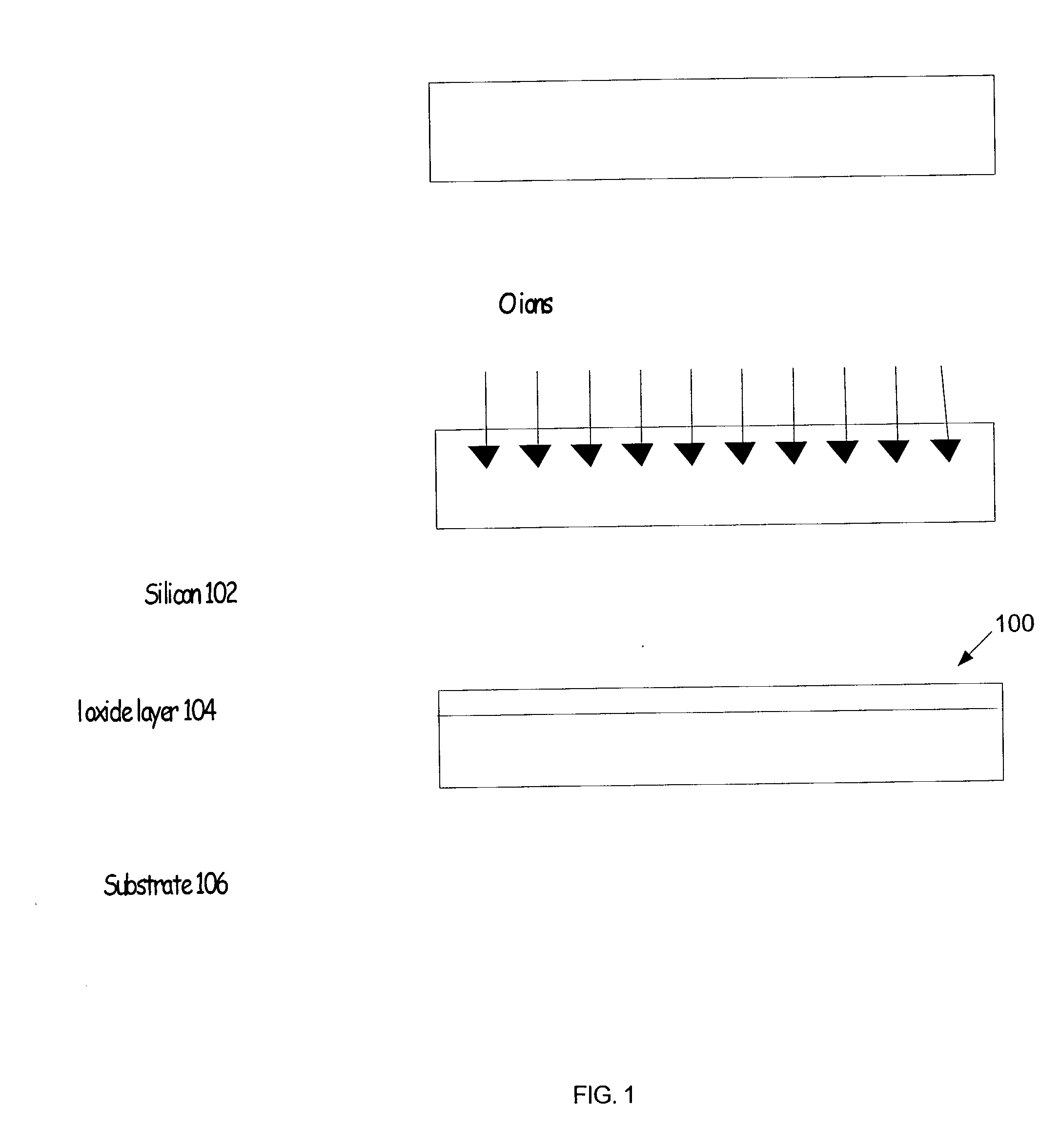
a technology of silicon on the surface of the silicon, applied in the direction of measurement devices, semiconductor/solid-state device testing/measurement, instruments, etc., can solve the problems of limiting the thickness of silicon layer 102 that can be achieved, the process has not been demonstrated for very thin films of silicon, and the effect of creating micro voids in silicon

Inactive Publication Date: 2004-06-10
INTEL CORP
View PDF11 Cites 3 Cited by
  • Summary
  • Abstract
  • Description
  • Claims
  • Application Information

AI Technical Summary

Problems solved by technology

This process has not been demonstrated for very thin films of silicon.
Lack of uniformity of silicon layer thickness, silicon layer defects, and process control may limit the thicknesses of silicon layer 102 that can be achieved.
Further, hydrogen implantation creates micro voids within silicon.
This process how

Method used


Image

  • Silicon-on-insulator devices and methods for fabricating the same
  • Silicon-on-insulator devices and methods for fabricating the same
  • Silicon-on-insulator devices and methods for fabricating the same

Examples


Embodiment Construction

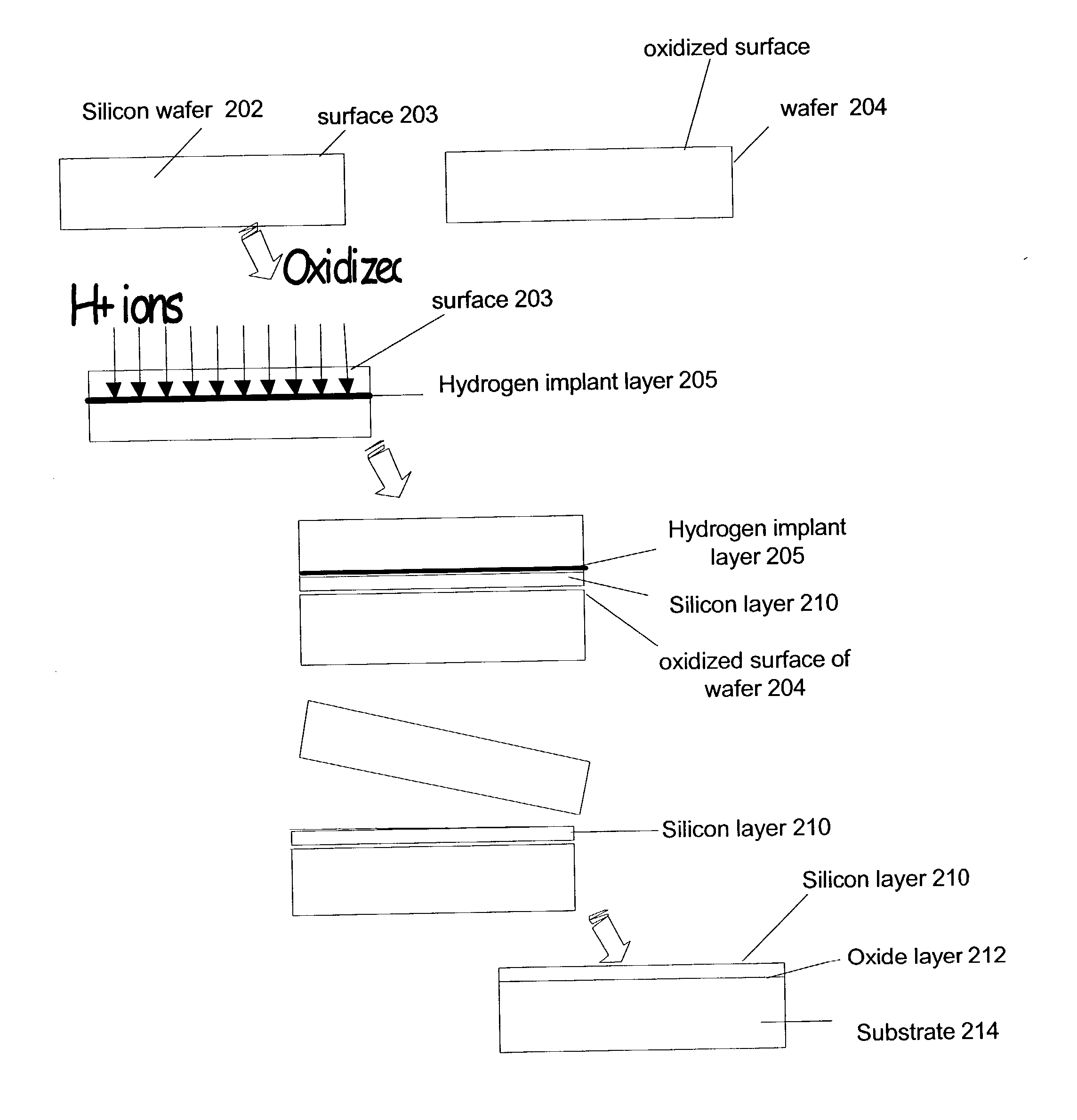
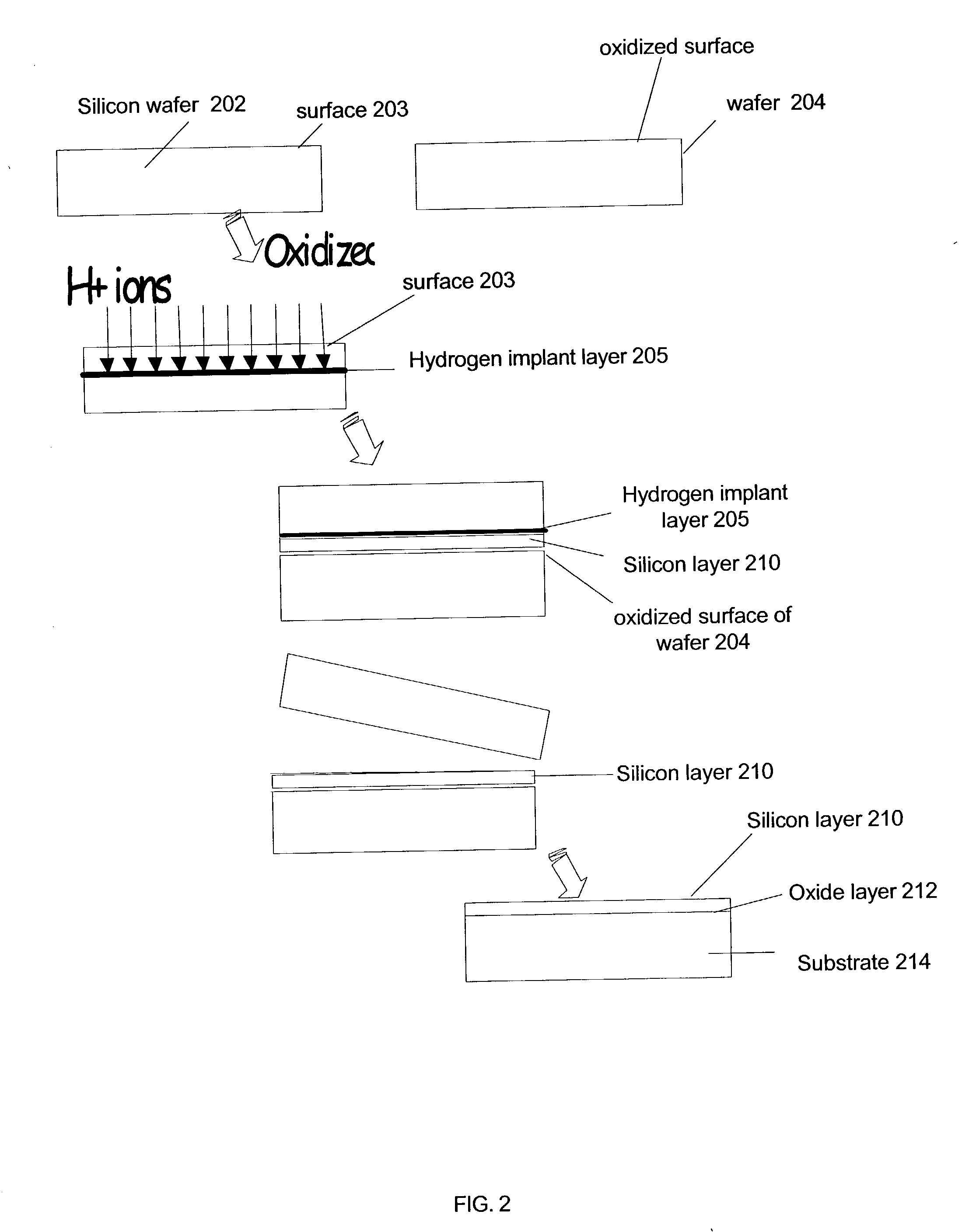
[0013] In accordance with an embodiment of the present invention, FIG. 3 depicts one possible implementation of a fabrication system 300 that can be used to construct SOI wafers such as an SOI wafer 330 of FIG. 4. As depicted in FIG. 4, SOI wafer 330 may include a silicon layer 410 formed over an oxide layer 420. Oxide layer 420 may be formed over substrate 430. Fabrication system 300 may utilize etch tool 310 and depth measurer 320 to adjust a thickness of the silicon layer 410 of SOI wafer 330. A control system 305 may be used to coordinate the actions of etch tool 310 and depth measurer 320. For example, control system 305 may control the amount the etch tool 310 and depth measurer 320 move across the surface of silicon layer 410 as well as the amount of silicon that etch tool 310 removes from silicon layer 410. For example, control system 305 may be implemented as any of or a combination of: hardwired logic, software stored by a memory device and executed by a microprocessor, fi...


PUM


Abstract

Techniques for local and selective thinning of silicon using a combination of real time metrology for film thickness measurement accompanied by local etching of the silicon to thin the silicon to the desired value. Etching is accomplished using a miniature plasma etcher with activated etch gases. The etch tool and the metrology tool are stepped across the wafer surface to achieve wafer level thinning of the top silicon.

Description

FIELD[0001] The subject matter disclosed herein generally relates to techniques to manufacture semiconductor devices.DESCRIPTION OF RELATED ART[0002] Silicon-on-insulator ("SOI") technology is an emerging technique for fabricating high-speed Metal-Oxide-Semiconductor (MOS) and Complementary Metal Oxide Semiconductor (CMOS) circuits in very large scale integrated (VLSI) circuits. An SOI wafer may have a thin single crystal layer of semiconductor material (e.g., silicon) formed on an insulator (e.g., a buried oxide film) that reduces capacitive coupling between the layer of semiconductor material and an underlying substrate material.[0003] One process to manufacture an SOI wafer is the Separation by Implantation of Oxygen (SIMOX) process. FIG. 1 depicts an example SIMOX fabrication process. The SIMOX process utilizes oxygen (0) ion implantation and annealing to form a buried oxide layer 104. The thickness of the silicon layer 102 may be controlled by controlling the depth that oxygen ...

Claims


Application Information

Patent Timeline
IPC IPC(8): H01L21/3065H01L21/66H01L21/762
CPCH01L21/3065H01L22/20H01L22/12H01L21/76254
Inventor RAVI, KRAMADHATI V.
Owner INTEL CORP
Why Eureka
Try Eureka