

Probe card for testing a semiconductor
a technology for semiconductors and probes, applied in electrical testing, measurement devices, instruments, etc., can solve problems such as and affecting the accuracy of the tes
- Summary
- Abstract
- Description
- Claims
- Application Information
AI Technical Summary
Benefits of technology
Problems solved by technology
Method used
Image

Examples
Embodiment Construction
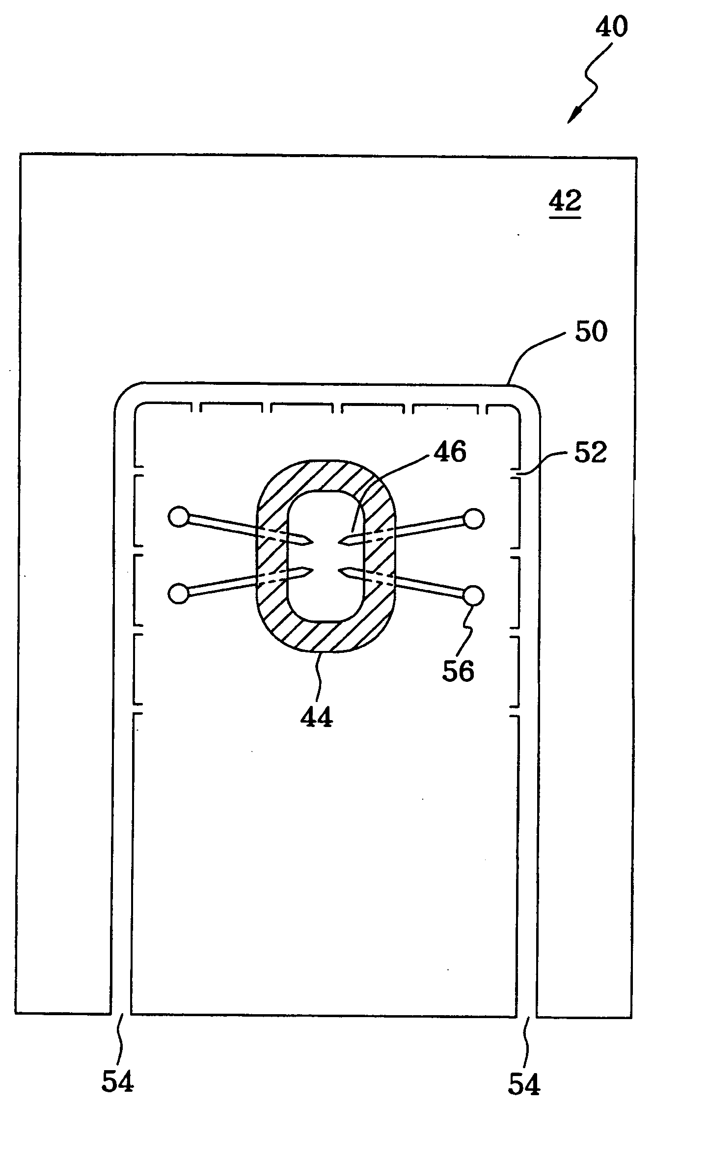
[0023] FIG. 4 is a top view of a probe card 40 according to the present invention. The probe card 40 comprises a circuit board 42, a circular supporter 44 positioned on the circuit board 42, a plurality of probe needles 46 positioned on the circular supporter 44, wires 48 connected to the end of the probe needle 46 and a flow line 50 positioned on the circuit board 42. The flow line 50 can be a guide tube, and the circuit board 42 and circular supporter 44 are made of ceramics that can sustain high temperature. The flow line 50 comprises two entrances 54 and a plurality of openings 52 toward to the circular supporter 44. The flow line 50 surrounds the circular supporter 44, the probe needles 46 and the wires 48.
[0024] FIG. 5 is a cross-sectional diagram showing the probe card 40 when applied in testing a semiconductor wafer 86 according to the present invention. There is a central opening 54 for an operator to visually inspect the relative distance of the probe needle 46 and the sem...
PUM
 Abstract
Description
Claims
Application Information