Crystal growth methods

a growth method and crystal technology, applied in the direction of polycrystalline material growth, crystal growth process, instruments, etc., can solve the problems of limiting the ability to produce calcium fluoride crystals suitable for optical lithography, high fluence damage, and fused silica, and achieve stable annealing/cooling process, high homogeneous index of refraction, and low stress birefringence

Inactive Publication Date: 2004-08-12
CORNING INC
View PDF11 Cites 12 Cited by
  • Summary
  • Abstract
  • Description
  • Claims
  • Application Information

AI Technical Summary

Benefits of technology

0015] Applicants have discovered an improved annealing approach to overcome the above-described problems presented by conventional multiple cooling rate annealing methods for CaF.sub.2 crystals. One aspect of the invention provides an in-situ annealing process in the growth furnace for crystals, and in particular, <111>- and <100>-grown calcium fluoride crystals so a highly homogenous index of refraction and low stress birefringence can be obtained. According to another aspect of the invention, a stable annealing/cooling process is provided that can consistently deliver an acceptable annealing result even with equipment and operation variability. In still another aspect of the invention, cooling conditions are provided that are specifically suitable for a post-grown crystal in a growth furnace so that the stress induced birefringence and the defects generated during the growth c...

Problems solved by technology

Semiconductor lithography equipment operating at 193 nm wavelengths commonly uses fused silica optical elements, but a limitation of fused silica is that it is damaged by high fluence at 193 nm.
However, current crystal growth and annealing processes lead to high residual stress in large calcium fluoride crystals, thus limiting the ability to produce calcium fluoride crystals suitable for optical lithography.
When used in an optical system, these stress induced effects can lead to wavefront errors, image degradation and birefringence, all of which are d...

Method used


Image

  • Crystal growth methods
  • Crystal growth methods
  • Crystal growth methods

Examples


Embodiment Construction

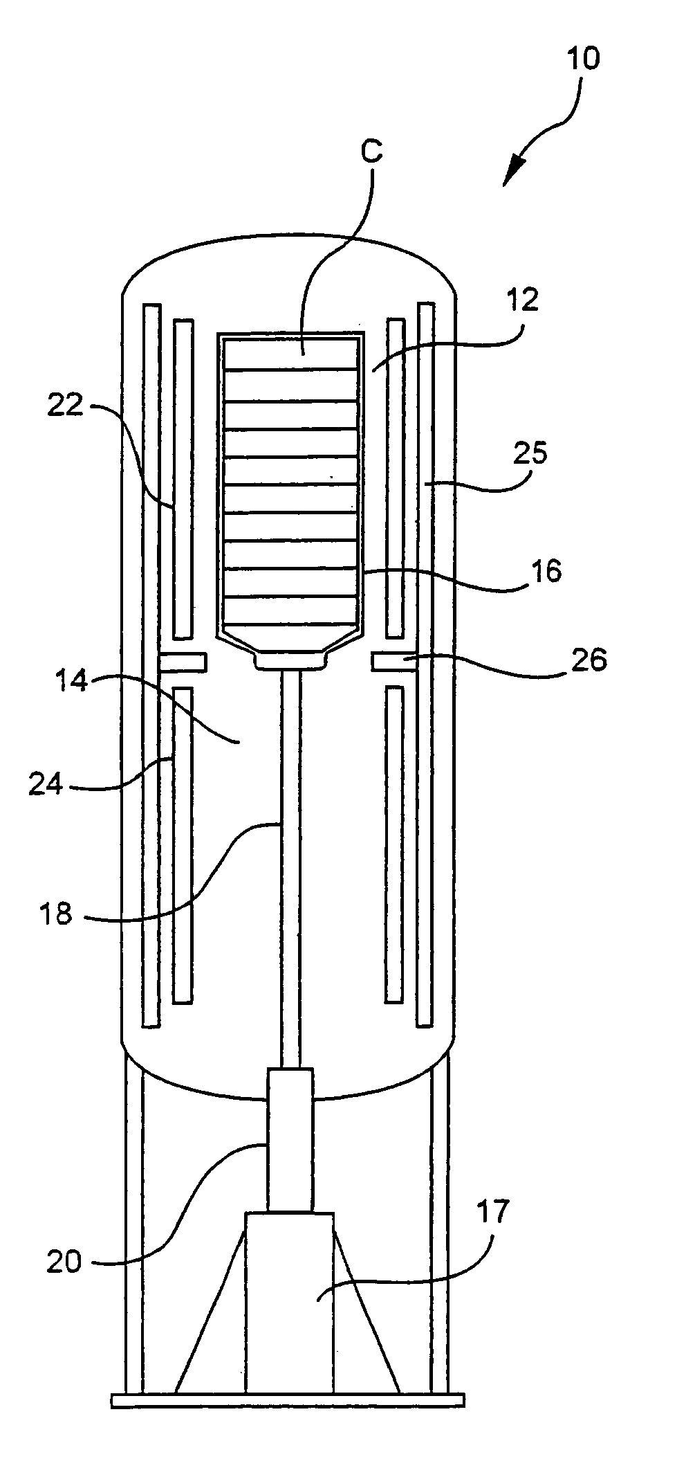
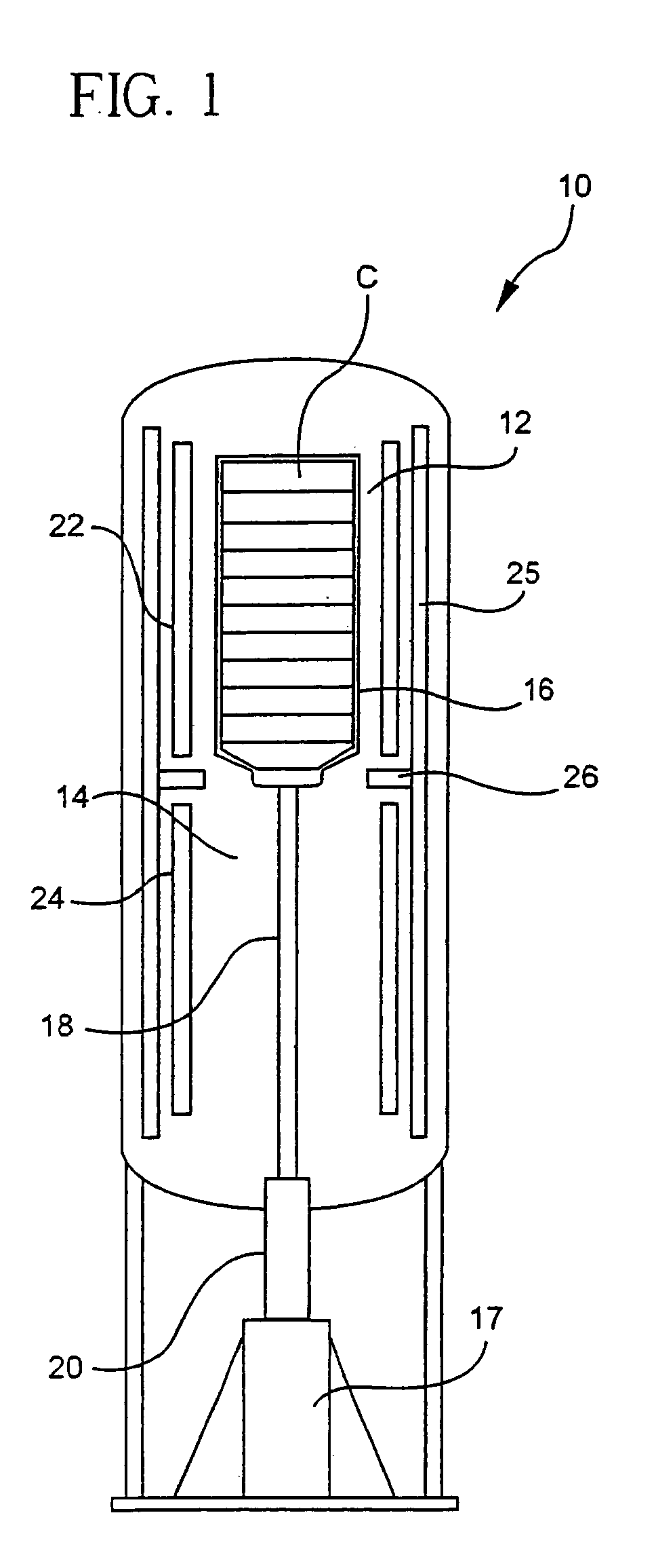
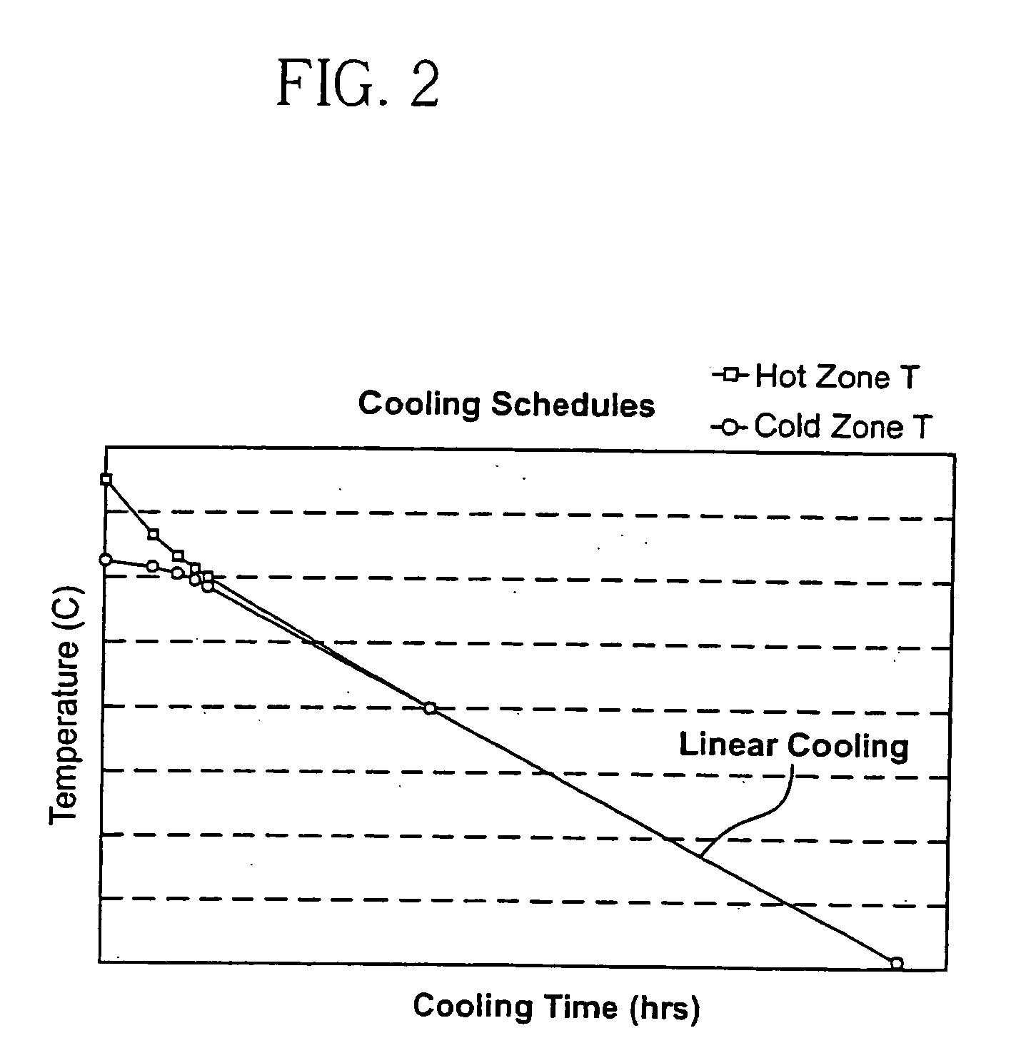
[0024] Experiments were carried out in a Bridgman-Stockbarger furnace for growing crystals having a or a orientation using two different annealing approaches. One annealing approach was the conventional multiple cooling rate method and the other was the substantially constant cooling rate approach according to the present invention. The experiments used equivalent heating-up profile and the growth conditions. The only difference between the two experiments was in the cooling portion of the processing. Actual experiments for the invented linear annealing profile were performed at a cooling rate of approximately 2.degree. C. / hr.

[0025] The conventional process consisted of a rapid cooling rate in the upper portion of the cycle (approximately 6.degree. C. / hour between about 1500.degree. C. to about 1100.degree. C.), a slow cooling rate in the middle portion of the cycle (1.5.degree. C. / hour between about 1100.degree. C. to about 750.degree. C.), an increased cooling rate of about 5.degr...


PUM


Abstract

The invention is directed to method of preparing metal fluoride single crystals and particularly to crystals where the metal is calcium, barium, magnesium or strontium, or a mixture thereof. The invention uses a decreasing fast cooling profile and an increasing slow cooling profile for the hot zone and the cold zone, respectively, after crystal formation during cooling from melt temperatures to a first temperature. A substantially constant cooling rate is then applied to the both zones during cooling from the first temperature to a final temperature, usually room temperature. It has been found that the substantially constant cooling rate during the annealing process results in crystals having improved homogeneity and birefringence.

Description

PRIORITY[0001] This application claims the priority of U.S. Provisional Application No. 60 / 442,195, filed Jan. 24, 2003, and titled "CRYSTAL GROWTH METHODS".[0002] This invention relates to crystal growth and annealing, and more specifically to methods for crystal growth and annealing that produce minimized residual stress and are suitable for production of calcium fluoride crystals.[0003] Metal fluoride crystals are used in various applications, for example, as optical elements in lithography equipment used in semiconductor processing. Semiconductor lithography equipment operating at 193 nm wavelengths commonly uses fused silica optical elements, but a limitation of fused silica is that it is damaged by high fluence at 193 nm. The next generation of semiconductor lithography is expected to use 157 nm wavelength illumination, and fused silica is quite opaque to 157 nm wavelength illumination.[0004] Calcium fluoride is a candidate material for use in optical elements in 193 nm and 15...

Claims


Application Information

Patent Timeline
IPC IPC(8): G02B1/02C30B11/00C30B29/12
CPCC30B11/00C30B29/12
Inventor LI, QIAOROSCH, WILLIAM R.SCHERMERHORN, PAUL M.
Owner CORNING INC
Why Eureka
Try Eureka