Device and method for producing single crystals by vapor deposition

a technology of single crystals and vapor deposition, which is applied in the direction of crystal growth process, polycrystalline material growth, gel state, etc., can solve the problems of limiting the duration of a continuous crystal growth process and thus the crystal length, the need to control the sublimation rate change, and the drift of sublimed species, so as to reduce the concentration of unwanted metallic impurities, slow down or eliminate the formation

Active Publication Date: 2005-01-06
NORSTEL
View PDF10 Cites 67 Cited by
  • Summary
  • Abstract
  • Description
  • Claims
  • Application Information

AI Technical Summary

Benefits of technology

[0018] In particular, it is an object of preferred embodiments of the invention to slow down or eliminate the formation of polycrystalline and other solid deposits downstream of the single crystal crystallization area to avoid a partial or complete obstruction of a susceptor exhaust path by a gas mixture fed to the crystallization area. A correlated purpose of preferred embodiments of the invention is to control the diameter of the growing single crystal and p

Problems solved by technology

Despite these achievements, there are however some challenges and limits in the sublimation technique.
For example, as long as no continuous feeding mechanism can be devised, the initial mass of the feedstock limits the duration of a continuous crystal growth process and thus the crystal length.
One difficulty may, for example, be the need to control a changing sublimation rate and a drift of the sublimed species stoichiometry during growth.
Instabilities in the source material supply and drifts of the temperature distribution in the source feedstock, for example, cause drifts of the growth rate and of the incorporation of doping species.
If not properly controlled, such drifts tend to adversely affect the yield of the crystal growth process.
Further downstream, as the temperatures decreases and the supersaturation increases, the less dense polycrystalline deposits grow even faster, eventually obstructing the gases outlet path within 2 to 4 hours.
If the pressure differential is allowed to reach a few mbars, a rapid deterioration of the polytype and the structural quality of the single crystal occurs.
The thermal properties of the insulating material are then rapidly deteriorating due to reaction with silicon, which forces the growth to be interrupted.
The parasitic deposition of polycrystalline solid phases thus leads to a catastrophic runaway of the system, forcing to terminate the growth process bef

Method used


Image

  • Device and method for producing single crystals by vapor deposition
  • Device and method for producing single crystals by vapor deposition
  • Device and method for producing single crystals by vapor deposition

Examples


Embodiment Construction

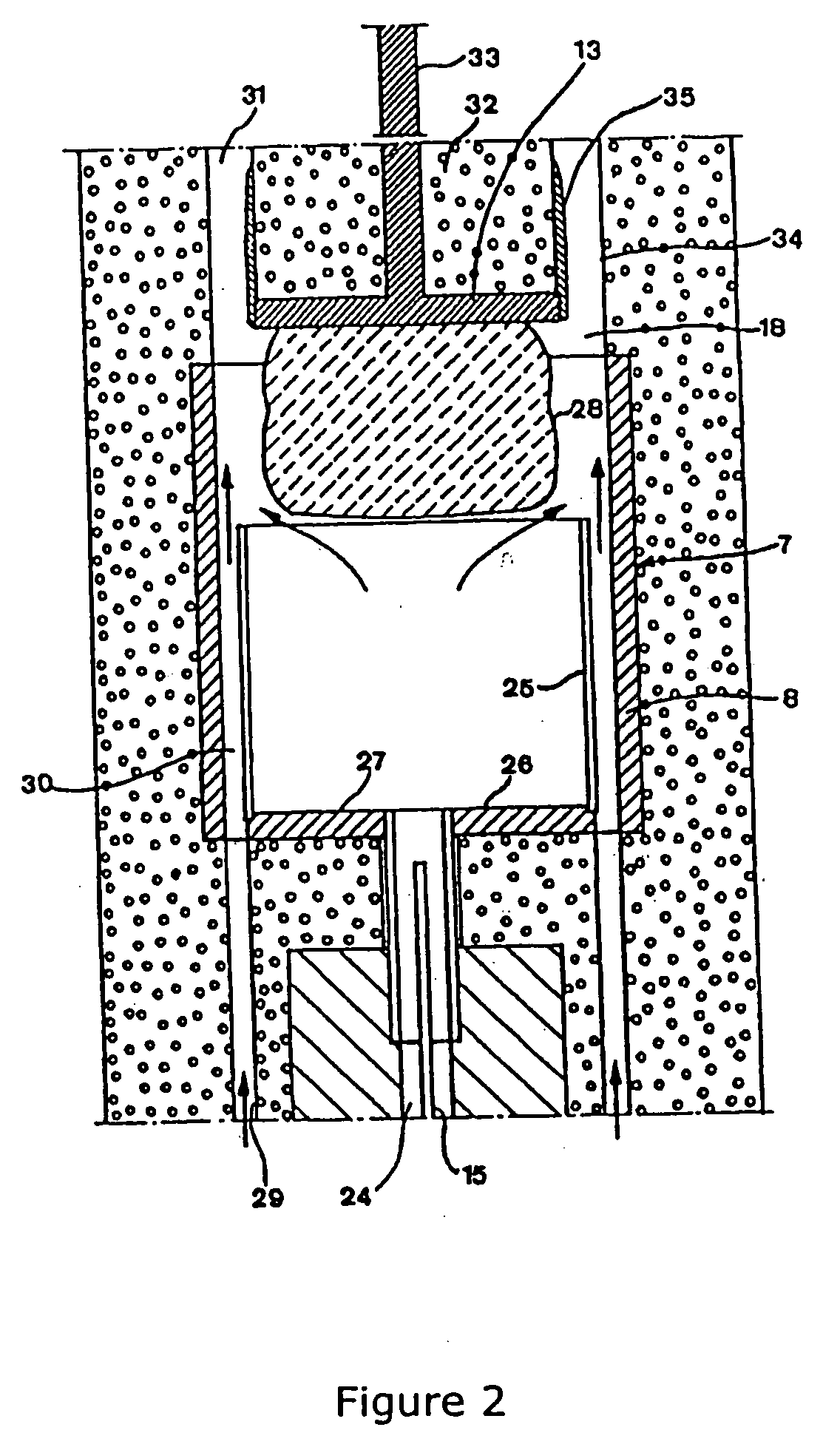
[0027]FIG. 3 schematically shows an improved device comprising a growth chamber of a HTCVD system based on the concepts described in the U.S. Pat. Nos. 5,704,985, 6,039,812 and 6,048,398. This device will also be described here as preferred embodiments of the device of the invention may have a similar principle construction as in the above mentioned documents but differ in the particular features and improvements described herein. The device of FIG. 3 is suited to grow single crystals of SiC or of a group-III nitride. Some parts are for the sake of simplicity schematized and it is obvious to a person skilled in the technical field that the device also comprises elements such as mass flow controllers, valves, pumps, control electronics, purifiers, a scrubbing system and other elements, as is common practice in CVD systems.

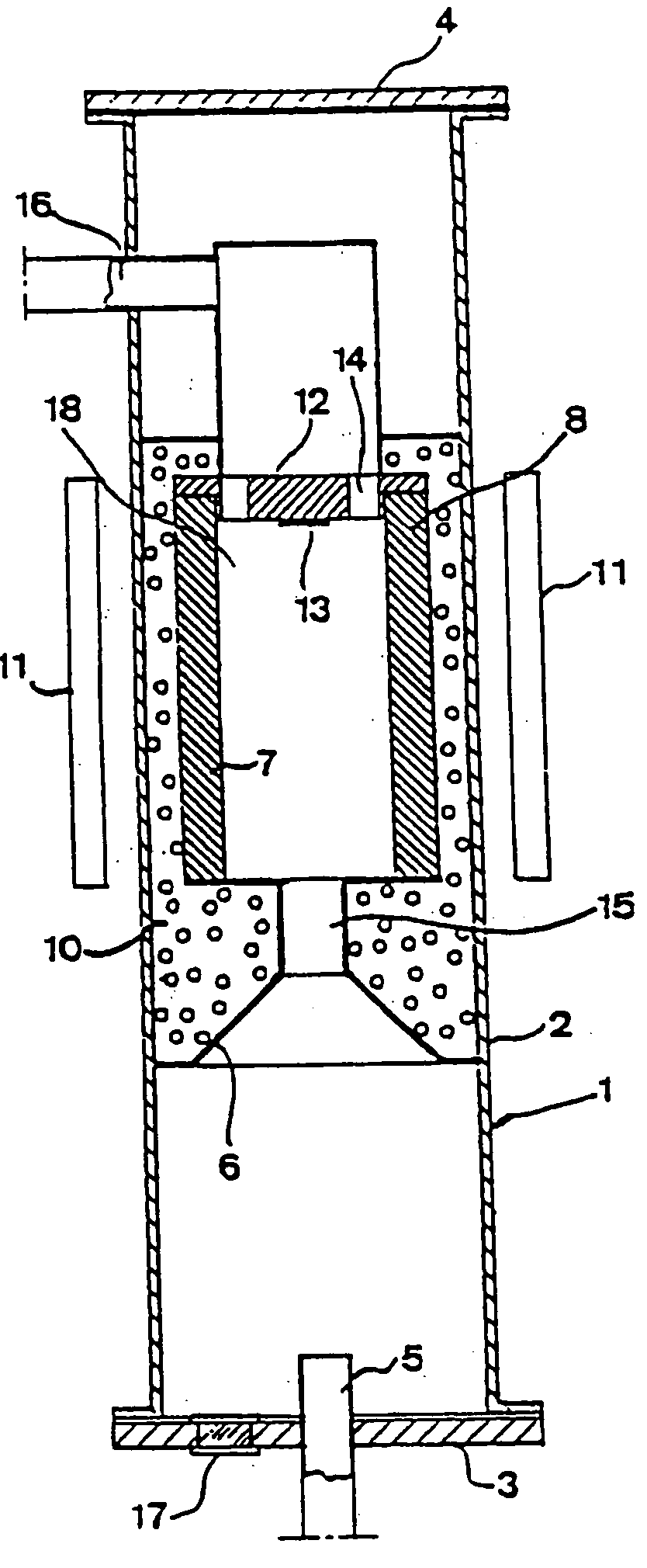
[0028] The high temperature chemical vapor deposition device comprises a casing 1 constituted, for example, of a single wall quartz tube 2 tightly mounted between ...


PUM


Abstract

A method and a device to grow from the vapor phase, a single crystal of either SiC, a group III-nitride, or alloys thereof, at a growth rate and for a period of time sufficient to produce a crystal of preferably several centimeters length. The diameter of the growing crystal may be controlled. To prevent the formation of undesirable polycrystalline deposits on surfaces in the downstream vicinity of the single crystal growth area, the local supersaturation of at least one component of the material grown is lowered by introducing a separate gas flow comprising at least one halogen element or a combination of said halogen and hydrogen species.

Description

FIELD OF THE INVENTION [0001] The present invention describes a device and a method to grow single crystals by high temperature deposition from a vapor phase. In particular the device can be used to produce large and high quality bulk crystals of a) silicon carbide, b) a group III-nitride, for example GaN or AlN, or c) an alloy of SiC and a group III-nitride. BACKGROUND AND PRIOR ART [0002] Wide band-gap semiconducting crystals such as silicon carbide (SiC), group III-nitrides e.g. gallium nitride (GaN) and aluminum nitride (AlN); offer several attractive electrical and physical properties for fast switching power devices and optoelectronic devices. These wide band gap semiconductors and their alloys also differentiate themselves from other important semiconductors, such as silicon and gallium arsenide, by the fact that they cannot at present be directly grown from a melt or a liquid solution under practically and economically interesting conditions. Instead, ingots of SiC, GaN or A...

Claims


Application Information

Patent Timeline
IPC IPC(8): C30B23/00C30B25/14C30B29/36C30B29/38C30B29/40C01B21/06
CPCC30B29/36Y10T117/1016C30B23/002C30B29/403
Inventor JANZEN, ERIKRABACK, PETERELLISON, ALEXANDRE
Owner NORSTEL
Why Eureka
Try Eureka