
Lithographic apparatus and device manufacturing method

a technology of lithographic apparatus and manufacturing method, which is applied in the direction of electrical apparatus, printing, instruments, etc., can solve the problem of not significantly increasing the processing time of the substrate, and achieve the improvement of the overlay accuracy of each part of the substrate, the increase of the apparatus, and the improvement of the overlap accuracy of each portion of the substrate.

Active Publication Date: 2005-01-13
ASML NETHERLANDS BV
View PDF33 Cites 404 Cited by
  • Summary
  • Abstract
  • Description
  • Claims
  • Application Information

AI Technical Summary

Benefits of technology

[0010] According to this embodiment, the throughput of the apparatus can be increased because the detector can inspect the complete substrate, or portions of the substrate, representative of the complete substrate. Then, the apparatus exposes the required pattern on the substrate by scanning the substrate relative to the apparatus in a single pass. This is especially beneficial in the manufacture of Flat Panel Displays, for example, in which the glass substrate being processed may be up to 2 m by 2 m or more in size.
[0023] Consequently, the pattern being projected onto the substrate can be adjusted to compensate for localized thermal expansion of the substrate, for example. The controller can further adjust the position of the pattern projected onto the substrate and / or the best focus image plane.

Problems solved by technology

Furthermore, since the substrate does not need to be transported to a separate alignment measuring center, the processing time of the substrate is not significantly increased.

Method used


Image

  • Lithographic apparatus and device manufacturing method
  • Lithographic apparatus and device manufacturing method
  • Lithographic apparatus and device manufacturing method

Examples


Embodiment Construction

[0035] Terminology

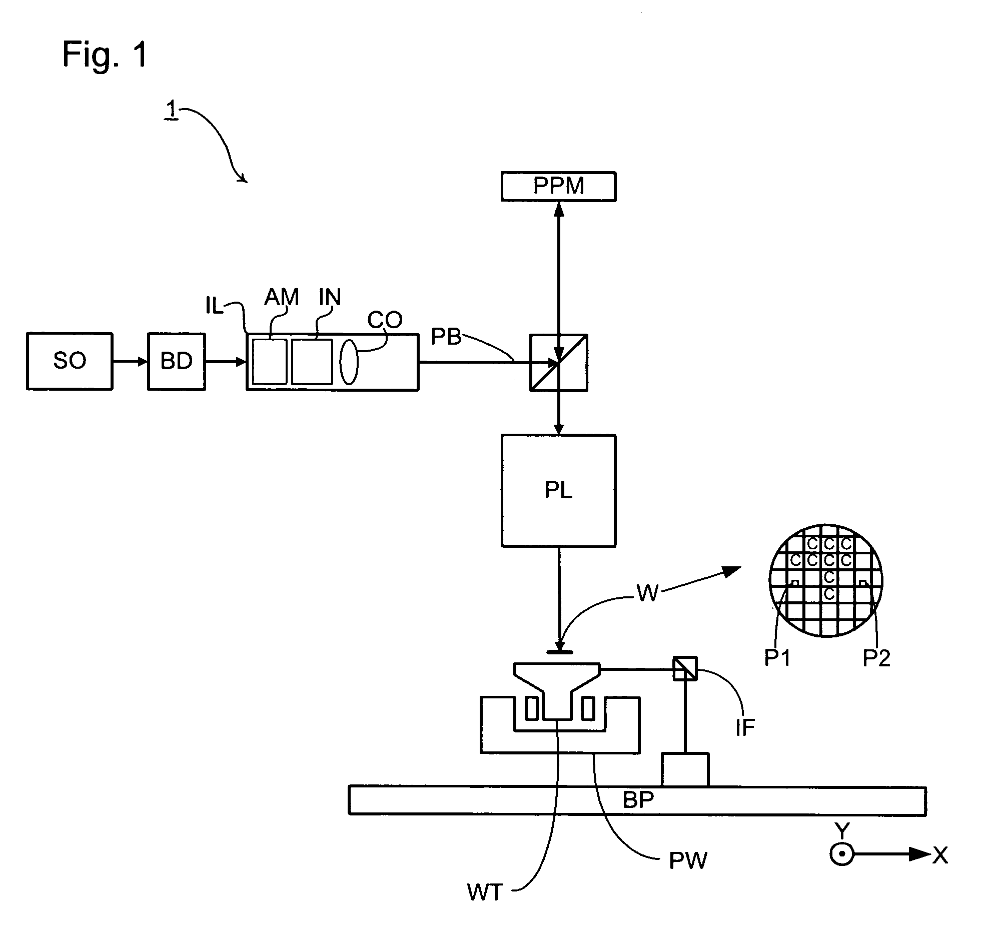
[0036] The term “array of individually controllable elements” as here employed should be broadly interpreted as referring to any means that can be used to endow an incoming radiation beam with a patterned cross-section, so that a desired pattern can be created in a target portion of the substrate; the terms “light valve” and “Spatial Light Modulator” (SLM) can also be used in this context. Examples of such patterning means include, but are not limited to, a programmable mirror array and a programmable liquid crystal device (LCD) array.

[0037] A programmable mirror array may comprise a matrix-addressable surface having a viscoelastic control layer and a reflective surface. The basic principle behind such an apparatus is that addressed areas of the reflective surface reflect incident light as diffracted light, whereas unaddressed areas reflect incident light as undiffracted light. Using an appropriate spatial filter, the undiffracted light can be filtered out of the...


PUM


Abstract

A lithographic apparatus in which alignment marks on the substrate are inspected during the exposure of the substrate to optimize the exposure conditions.

Description

BACKGROUND OF THE INVENTION [0001] 1. Field of the Invention [0002] The present invention relates to a lithographic apparatus and a device manufacturing method. [0003] 2. Related Art [0004] A lithographic apparatus is a machine that applies a desired pattern onto a target portion of a substrate. Lithographic apparatus can be used, for example, in the manufacture of integrated circuits (ICs), flat panel displays and other devices involving fine structures. In a conventional lithographic apparatus, a patterning means, which is alternatively referred to as a mask or a reticle, may be used to generate a circuit pattern corresponding to an individual layer of the IC (or other device), and this pattern can be imaged onto a target portion (e.g., comprising part of one or several dies) on a substrate (e.g., a silicon wafer or glass plate) that has a layer of radiation-sensitive material (resist). Instead of a mask, the patterning means may comprise an array of individually controllable elem...

Claims


Application Information

Patent Timeline
IPC IPC(8): G03F7/20G03F9/00H01L21/027
CPCG03F7/70291G03F7/70791G03B27/53G03F9/7026G03F9/7003G03F7/70216G03F7/70716G03F9/7073G03F9/7088
Inventor GEORGE, RICHARD ALEXANDERGUI, CHENG-QUNJAGER, PIETER WILLEM HERMAN DELEEUWEN, ROBBERT EDGAR VANBURGHOOM, JACOBUS
Owner ASML NETHERLANDS BV
Features
  • Generate Ideas
  • Intellectual Property
  • Life Sciences
  • Materials
  • Tech Scout
  • Unparalleled Data Quality
  • Higher Quality Content
  • 60% Fewer Hallucinations
Learn More