Interlayer dielectric and pre-applied die attach adhesive materials

a technology of adhesive materials and dielectric layers, applied in the direction of metal layered products, solid-state devices, electrical devices, etc., can solve the problems of little progress, cross-talk, and internal package reduction, and achieve the effect of avoiding dispensing, handling and storage problems

Inactive Publication Date: 2005-01-13
HENKEL CORP
View PDF22 Cites 29 Cited by
  • Summary
  • Abstract
  • Description
  • Claims
  • Application Information

AI Technical Summary

Benefits of technology

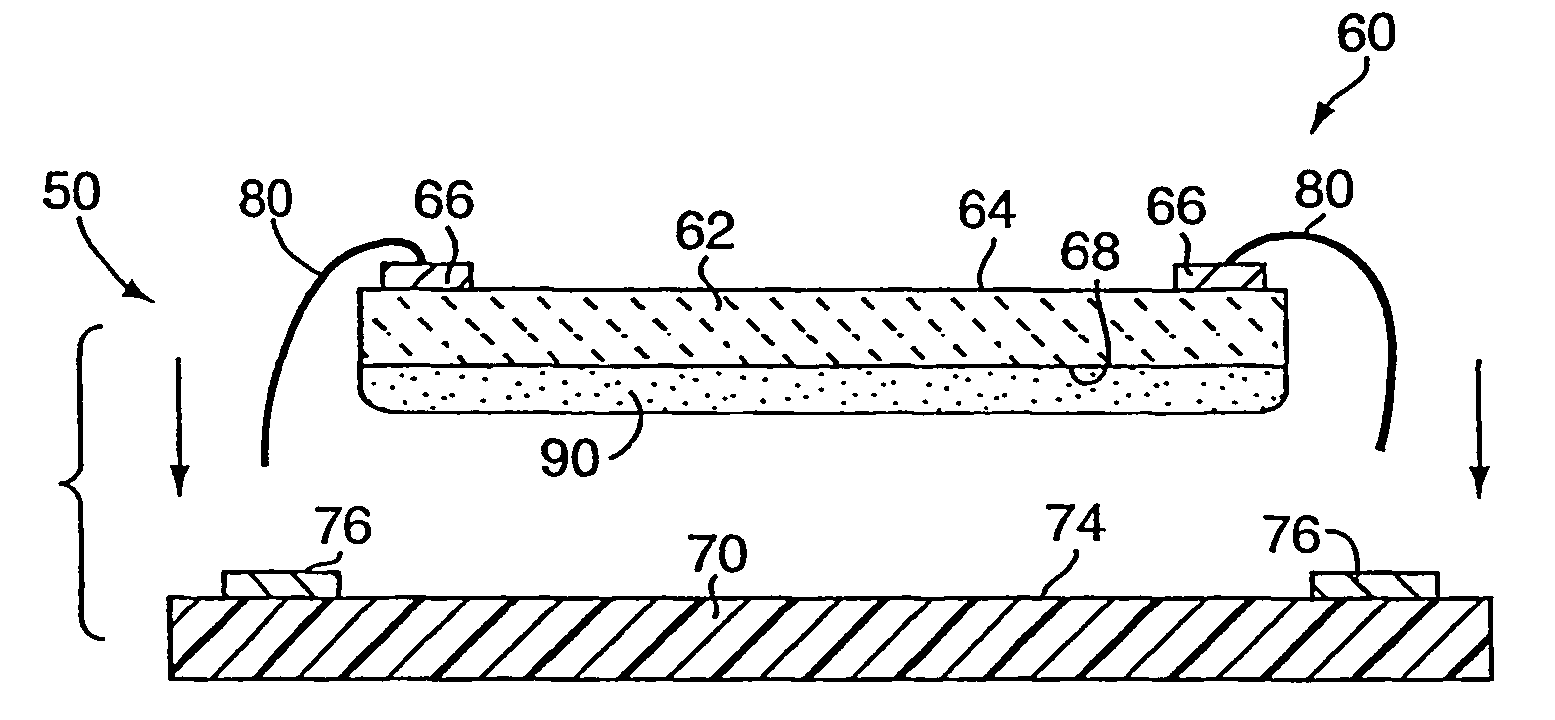
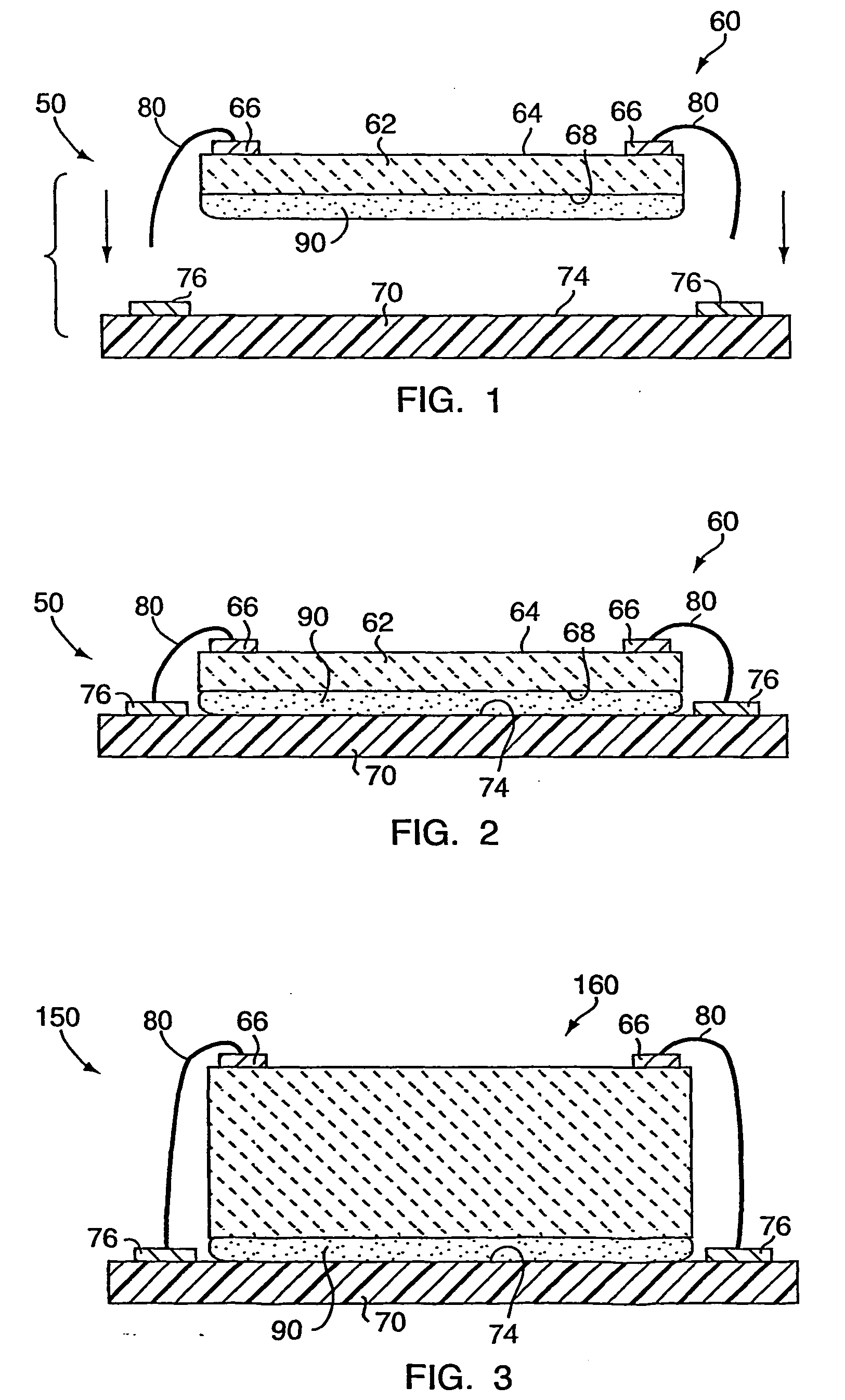
The present invention provides advantages relating to the avoidance of dispensing, handling and storage issues for the end user seeking to assemble in particular microelectronic devices using a semiconductor chip having an adhesive material pre-applied to a surface thereof.

Problems solved by technology

Cross talk is a common problem in integrated circuit manufacturing, as it causes malfunctions in the circuit.
Little progress has been reported to date, however, at reducing the internal package stresses that lead to the ILD cracking failures.
Pre-applied adhesives themselves are not a new commercial product.
However, to date there has not been an article of manufacture placed in commerce, such as a semiconductor chip or a semiconductor wafer, with a die attach adhesive material pre-applied thereon for application without the intermediate process steps attendant with a flowable die attach adhesive material, particularly where the reactive component of the adhesive material is based in whole or in part on a bismaleimide or for more extreme environments where the reactive component of the die attach adhesive material is based in whole or in part on a benzoxazine.

Method used


Image

  • Interlayer dielectric and pre-applied die attach adhesive materials
  • Interlayer dielectric and pre-applied die attach adhesive materials
  • Interlayer dielectric and pre-applied die attach adhesive materials

Examples


examples

In a first example, a die attach adhesive material was prepared for pre-application to a semiconductor chip using the styrene-butadiene block copolymer, KRATON D-1102, as a thermoplastic elastomeric component, and octadecylmaleimide and X-BMI (the 1,20-bismaleimido derivative of 10,11-dioctyl-eicosane) as maleimides. The die attached adhesive material for pre-application was prepared from the components recited below in Table 1.

TABLE 1Octadecylmaleimide 1.0 gKRATON D-1102 2.5 gX-BMI1 1.5 gRICON 1302 0.2 gSilane coupling agent3 0.2 gDicumyl peroxide0.05 gXylene 5.0 gTEFLON filler 6.9 g

1X-BMI (the 1,20-bismaleimido derivative of 10,11-dioctyl-eicosane), was prepared according to the procedure set forth in U.S. Pat. No. 5,973,166, the disclosure of which is hereby expressly incorporated herein by reference.

2Polybutadiene 20% grafted with maleic anhydride (Sartomer)

3Proprietary silane-containing coupling agent.

Octadecylmaleimide was dissolved in xylene, and KRATON D-1102 was adde...


PUM

PropertyMeasurementUnit
melting pointaaaaaaaaaa
temperatureaaaaaaaaaa
thermoplasticaaaaaaaaaa

Abstract

The present invention relates to interlayer dielectric materials and pre-applied die attach adhesives, more specifically pre-applied die attach adhesives (such as wafer and other substrate-applied die attach adhesives), methods of applying the interlayer dielectric materials onto substrates to prepare low K dielectric semiconductor chips, methods of applying the pre-applied die attach adhesives onto wafer and other substrate surfaces, and assemblies prepared therewith for connecting microelectronic circuitry.

Description

BACKGROUND OF THE INVENTION 1. Field of the Invention The present invention relates to interlayer dielectric materials and pre-applied die attach adhesives, more specifically pre-applied die attach adhesives (such as wafer and other substrate-applied die attach adhesives), methods of applying the interlayer dielectric materials onto substrates to prepare low K dielectric semiconductor chips, methods of applying the pre-applied die attach adhesives onto wafer and other substrate surfaces, and assemblies prepared therewith for connecting microelectronic circuitry. 2. Brief Description of Related Technology Bismaleimides occupy a prominent position in the spectrum of thermosetting resins, and a number of bismaleimides are commercially available. Bismaleimides have been used for the production of moldings and adhesive joints, heat-resistant composite materials, and high temperature coatings. More recently, Henkel Loctite Corporation has commercialized a number of products based in p...

Claims


Application Information

Patent Timeline
Patent Type & Authority Applications(United States)
IPC IPC(8): C09J11/06C08L79/08C09J5/06C09J135/00C09J153/00C09J163/00C09J181/04H01L21/52H01L21/58H01L21/768H01L21/98H01L23/522H01L25/065
CPCC08L79/08C08L79/085C09J5/06C09J2479/00H01L24/83H01L24/85H01L25/0657H01L25/50H01L2224/274H01L2224/32145H01L2224/32225H01L2224/48091H01L2224/48227H01L2224/73265H01L2224/83191H01L2224/83192H01L2224/83856H01L2224/8388H01L2224/85H01L2924/01002H01L2924/01004H01L2924/01005H01L2924/01006H01L2924/01011H01L2924/01012H01L2924/01013H01L2924/01014H01L2924/01015H01L2924/01018H01L2924/01027H01L2924/01028H01L2924/01029H01L2924/01032H01L2924/01033H01L2924/01039H01L2924/01046H01L2924/01047H01L2924/01051H01L2924/01057H01L2924/01074H01L2924/01077H01L2924/01078H01L2924/01079H01L2924/01082H01L2924/07802H01L2924/14H01L24/27H01L24/29H01L24/32H01L2224/2919H01L2924/00014H01L2924/01019H01L2924/01023H01L2924/01024H01L2924/014H01L2924/0665H01L2225/0651H01L2225/06506H01L2225/06568H01L2924/10253Y10T428/24917Y10T428/12562Y10T428/12569H01L2224/78H01L2924/00H01L2924/3512H01L2924/00012H01L24/48H01L24/73H01L2924/12042H01L2924/15787H01L2924/15788Y10T428/31663H01L2224/45099H01L21/31H01L21/52H01L23/12H01L29/02
Inventor SANTOS, BENEDICTO DE LOSHUNEKE, JAMES T.LIU, PUWEIYANG, KANG
Owner HENKEL CORP
Why Eureka
Try Eureka