Apparatuses for treating pluralities of discrete semiconductor substrates; and methods for treating pluralities of discrete semiconductor substrates

a technology of discrete semiconductor substrates and apparatuses, which is applied in the direction of crystal growth process, photosensitive materials, instruments, etc., can solve the problems of difficult control of reactions, and difficult to form uniform layers over multiple exposed surfaces of one or more semiconductor substrates with cvd

Inactive Publication Date: 2005-01-13
DEAN TRUNG TRI +3
View PDF37 Cites 74 Cited by
  • Summary
  • Abstract
  • Description
  • Claims
  • Application Information

AI Technical Summary

Benefits of technology

[0008] In one aspect, the invention encompasses a method for treating a plurality of discrete semiconductor substrates. The discrete semiconductor substrates are placed within a reactor chamber. While the substrates are within the chamber, they are simultaneously exposed to one or more of H, F and Cl to remove native oxide (such can be considered an in situ cleaning of th...

Problems solved by technology

Among the disadvantages of chemical vapor deposition is that it can be difficult to control reactions between the reactants provided in a chamber, and accordingly various side-reactions can occur to generate contaminants.
Additionally, it can be difficult to form a uniform layer over multiple exposed surfaces of one or more semiconductor substrates with CVD.
The deposition of CVD material can be faster in various regions of semiconductor typography than other regions, leading to non-uniformity in a thickness of the deposited material across various expo...

Method used


Image

  • Apparatuses for treating pluralities of discrete semiconductor substrates; and methods for treating pluralities of discrete semiconductor substrates
  • Apparatuses for treating pluralities of discrete semiconductor substrates; and methods for treating pluralities of discrete semiconductor substrates
  • Apparatuses for treating pluralities of discrete semiconductor substrates; and methods for treating pluralities of discrete semiconductor substrates

Examples


Embodiment Construction

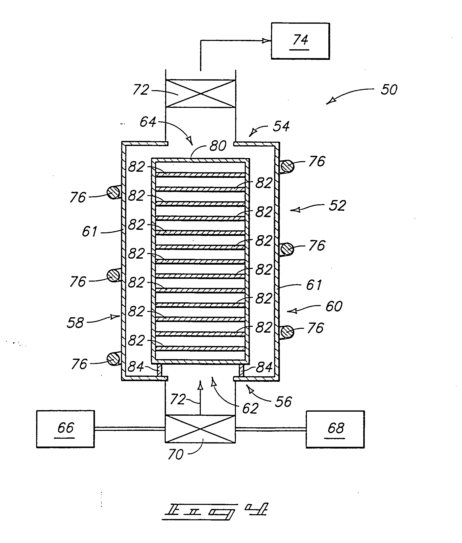
[0019] In particular aspects, the present application pertains to atomic layer deposition (ALD) technology. ALD technology typically involves formation of successive atomic layers on a substrate. Such layers may comprise, for example, an epitaxial, polycrystalline, and / or amorphous material. ALD may also be referred to as atomic layer epitaxy, atomic layer processing, etc.

[0020] The deposition methods herein are described in the context of formation of materials on one or more semiconductor substrates. In the context of this document, the term “semiconductor substrate” or “semiconductive substrate” is defined to mean any construction comprising semiconductive material, including, but not limited to, bulk semiconductive materials such as a semiconductive wafer (either alone or in assemblies comprising other materials thereon), and semiconductive material layers (either alone or in assemblies comprising other materials). The term “substrate” refers to any supporting structure, includ...


PUM

PropertyMeasurementUnit
Fractionaaaaaaaaaa
Fractionaaaaaaaaaa
Fractionaaaaaaaaaa

Abstract

The invention includes a method for treating a plurality of discrete semiconductor substrates. The discrete semiconductor substrates are placed within a reactor chamber. While the substrates are within the chamber, they are simultaneously exposed to one or more of H, F and Cl to remove native oxide. After removing the native oxide, the substrates are simultaneously exposed to a first reactive material to form a first mass across at least some exposed surfaces of the substrates. The first reactive material is removed from the reaction chamber, and subsequently the substrates are exposed to a second reactive material to convert the first mass to a second mass. The invention also includes apparatuses which can be utilized for simultaneous ALD treatment of a plurality of discrete semiconductor substrates.

Description

TECHNICAL FIELD [0001] The invention pertains to methods for treating pluralities of discrete semiconductor substrates to form layers of material over the substrates. In particular applications, the invention pertains to atomic layer deposition of materials over semiconductor substrates. The invention also pertains to apparatuses which can be utilized during treatment of a plurality of discrete semiconductor substrates. BACKGROUND OF THE INVENTION [0002] It is frequently desired to form high quality layers of material over semiconductor substrates during semiconductor device fabrication. Among the materials which can be included in such layers are tantalum pentoxide, titanium nitride, titanium silicon nitride, tantalum nitride, tantalum silicon nitride, titanium silicide, tantalum silicide, tungsten nitride, aluminum oxide, hafnium oxide, zirconium oxide, silicon nitride, silicon dioxide, elemental tungsten and elemental titanium. Numerous methods have been developed for forming lay...

Claims


Application Information

Patent Timeline
IPC IPC(8): C23C16/02C23C16/44C23C16/455C23C16/54C30B25/02H01L21/285H01L21/306H01L21/314H01L21/316H01L21/318H01L21/768
CPCC23C16/0236C23C16/0245C23C16/45546C23C16/54C30B25/02H01L21/02046H01L21/76888H01L21/3144H01L21/31604H01L21/31683H01L21/3185H01L21/76841H01L21/76856H01L21/28562H01L21/02211H01L21/02326H01L21/0228H01L21/0214H01L21/02164H01L21/0217H01L21/02142H01L21/02175
Inventor DEAN, TRUNG TRIBREINER, LYLE D.PING, ER-XUANZHENG, LINGYI A.
Owner DEAN TRUNG TRI
Why Eureka
Try Eureka