Photovoltaic converter

a photovoltaic converter and converter technology, applied in the field of photovoltaic converters, can solve the problems of new defects, increased carrier recombination loss, and power generation efficiency drop, and achieve the effect of reducing reflection loss and increasing power generation ra

Inactive Publication Date: 2005-01-20
TOYOTA JIDOSHA KK
View PDF9 Cites 28 Cited by
  • Summary
  • Abstract
  • Description
  • Claims
  • Application Information

AI Technical Summary

Benefits of technology

[0018] An object of the present invention is to provide a photovoltaic converter which maintains the function of the protective film, simultaneously reduces the reflection loss and carrier recombination loss, and raises the power generation rate.
[0020] Further, according a second embodiment of the first aspect of the invention, there is provided a photovoltaic converter formed on a semiconductor substrate and provided on its light receiving surface with a silicon nitride film as a protective film / antireflection film, wherein an Si—H2 / Si—H bond ratio is increased and a content of hydrogen or a halogen is decreased or a ratio of Si content / N content is increased at a boundary region of the silicon nitride film with the semiconductor substrate compared with other portions so as to maintain a refractive index at the boundary region equal to the other portions.
[0021] Further, according a third embodiment of the first aspect of the invention, there is provided a photovoltaic converter formed on a semiconductor substrate and provided on its light receiving surface with a silicon nitride film as a protective film / antireflection film, wherein an N—H / Si—H bond ratio is increased and a content of hydrogen or a halogen is reduced or a ratio of Si content / N content is increased at a boundary region of the silicon nitride film with the semiconductor substrate compared with other portions so as to maintain a refractive index at the boundary region equal to the other portions.

Problems solved by technology

However, if directly forming a thin film of TiO2 or ZnS on the surface of a Ge or other semiconductor substrate, a large amount of defects will remain at the surface of the semiconductor substrate or elements serving as sources of contamination will diffuse at the surface of the semiconductor substrate to cause new defects.
As a result, the concentration of defects becoming carrier recombination sites will become higher near the light receiving surface, the carrier recombination loss will increase, and the power generation efficiency will fall.
However, if a silicon nitride film contains a large content of hydrogen, its function as a protective film drops.
If the hydrogen content becomes greater, however, the refractive index of the silicon nitride film becomes smaller, so there is the problem that the refractive index would differ between the boundary region with the large hydrogen content and the other locations and therefore the antireflection effect would end up falling.
Use of silicon nitride as the bottommost layer film is therefore not possible.
However, the TiO2, ZnS, or other film used as the bottommost layer film R1 has a small effect of reduction of the dangling bonds of the surface of the semiconductor substrate as compared with an SiNx film R2 or SiO2 film R3, so an effect of reduction of the carrier recombination loss due to the reduction of the defects cannot be obtained.
However, the bottommost layer film constituted by the silicon nitride film R2 in the stacked structure has a refractive index lower than the high refractive index film R1 directly above it, so there is the problem of a drop in the antireflection effect.
In the final analysis, in the related art, it was not possible to maintain the function of the protective film, simultaneously reduce the reflection loss and carrier recombination loss, and raise the power generation rate.

Method used


Image

  • Photovoltaic converter
  • Photovoltaic converter
  • Photovoltaic converter

Examples


example 1

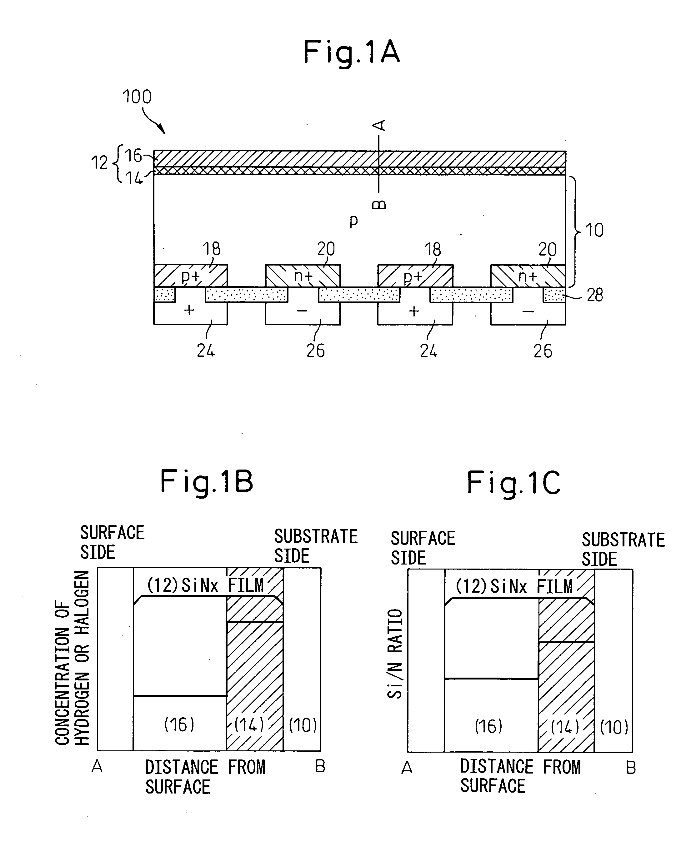
[0065]FIGS. 1A to 1C show an example of a photovoltaic converter according to the first embodiment of the first aspect of the invention. FIG. 1A is a cross-sectional view of the photovoltaic converter, FIG. 1B shows the profile of concentration of hydrogen or a halogen along line A-B of the same, and FIG. 1C shows the profile of the Si concentration / N concentration ratio.

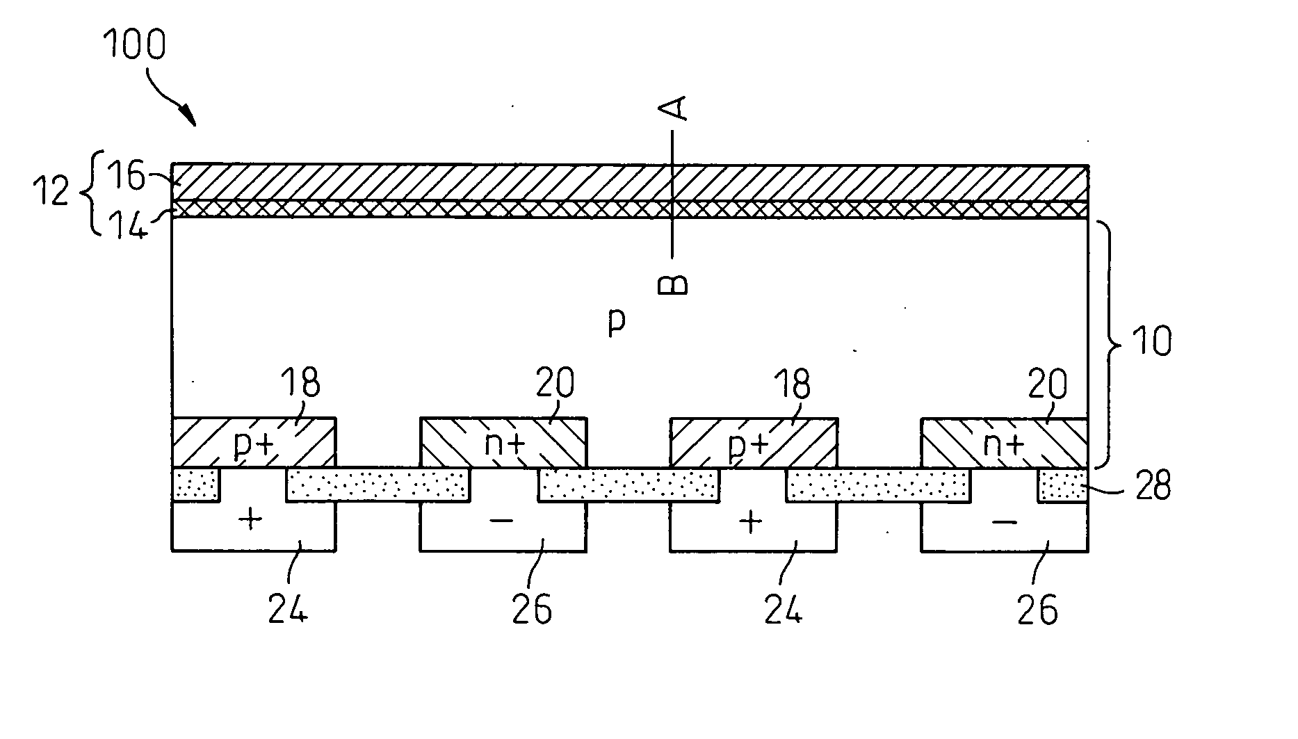
[0066] As shown in FIG. 1A, the photovoltaic converter 100 of the present invention is formed on a p-type semiconductor substrate 10 and is provided on its light receiving surface (top surface in figure) with a protective film / antireflection film 12 made of silicon nitride. The back surface side end (bottom end in the figure) of the semiconductor substrate 10 is formed with a p+ layer 18 and n+ layer 20 as carrier diffusion layers by diffusion. These are connected to the positive and negative outside output electrodes 24 and 26. The back surface at other than the connection positions of the carrier polarization lay...

example 2

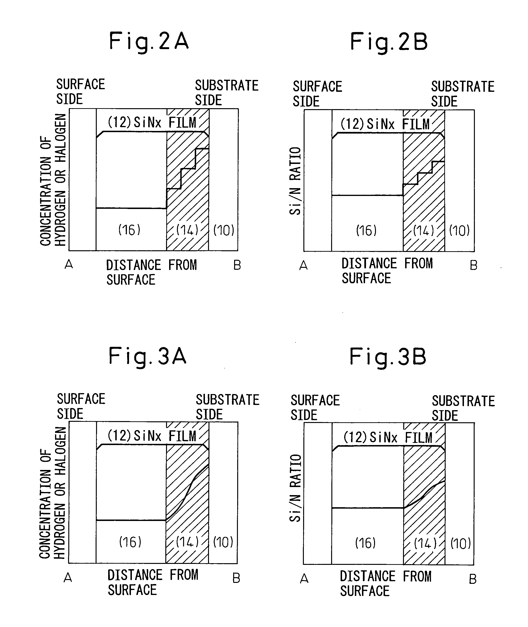
[0095] In Example 1, the content of hydrogen or a halogen (means X) and the ratio of the Si content / N content (means Y) were made constant profiles over the entire region of the boundary region 14, but the invention is not particularly limited to this. The means X and the means Y should be combined so that the refractive index inside the boundary region 14 is maintained equal to the other portions 16 (constant over entire boundary region 14). That is, the two means should balanced or combined so that the change in the refractive index due to the means X and the change in the refractive index due to the means Y cancel each other out to give a substantially zero change.

[0096]FIGS. 2A and 2B show preferable examples of profiles. The profiles increase stepwise from the surface side to the substrate 10 side in accordance with the content of hydrogen or a halogen (means X) in FIG. 2A and the ratio of the Si content / N content (means Y) in FIG. 2B. Due to this, the internal stress in the s...

example 3

[0120] In this example, as shown in FIGS. 3A and 3B, the content of the hydrogen or a halogen (means X) (FIG. 3A) and the ratio of the Si content / N content (means Y) (FIG. 3B) are continuously increased from the surface side (A side) to the substrate side (B side) in profile.

[0121] By adopting this continuous increase profile, the effect of change due to the step-wise increase profile of Example 2 is further enhanced. That is, the internal stress of the silicon nitride film 12 is further reduced so that (a) the effect of prevention of peeling of the silicon nitride film 12 due to the heat treatment in the device fabrication process is further enhanced and simultaneously (b) the effect of reduction of defects at the surface of the substrate 10 contiguous with the silicon nitride film 12 is further enhanced.

[0122] As a result, (a) the improvement in the production yield due to the prevention of peeling of the silicon nitride film 12 and the reduction in the production costs due to t...


PUM


Abstract

A photovoltaic converter, maintaining the function of a protective film, simultaneously reducing the reflection loss and carrier recombination loss, and raising the power generation efficiency, formed on a semiconductor substrate and provided on its light receiving surface with a silicon nitride film as a protective film / antireflection film, wherein a content of hydrogen or a halogen is increased and a ratio of Si content / N content is increased at a boundary region of the silicon nitride film with the semiconductor substrate compared with other portions so as to maintain a refractive index at the boundary region equal to the other portions.

Description

BACKGROUND OF THE INVENTION [0001] 1. Field of the Invention [0002] The present invention relates to a photovoltaic converter formed on a semiconductor substrate and provided on its light receiving surface with a silicon nitride film etc. as a protective film / antireflection film, more particularly relates to a photovoltaic converter reduced in reflection loss and carrier recombination loss. [0003] 2. Description of the Related Art [0004] In recent years, as devices for directly obtaining electrical energy from heat sources, attention is being focused on thermophotovoltaics (TPV). The principle is to heat a light emitter by a heat source to cause the emission of radiant light from the light emitter and to project this radiant light on a photovoltaic converter (PV cell) to obtain electrical energy. As the heat source, the exhaust heat from various types of plants, boilers, heaters, etc. or the heat of combustion of fossil fuels is used. [0005] TPV uses radiant light obtained in partic...

Claims


Application Information

Patent Timeline
Patent Type & Authority Applications(United States)
IPC IPC(8): H01L31/04H01L25/00H01L31/00H02N6/00
CPCY02E10/50H01L31/02168
Inventor NAGASHIMA, TOMONORIKAWAGUCHI, KAZUYOSHI
Owner TOYOTA JIDOSHA KK
Why Eureka
Try Eureka