Thin film transistor formed on a transparent substrate

a technology of thin film transistors and transparent substrates, applied in the direction of manufacturing tools, radiofrequency control devices, instruments, etc., can solve the problems of reducing throughput, increasing and affecting the quality of the substrate, so as to achieve high throughput, simple configuration, and increase the number of process steps.

Inactive Publication Date: 2005-01-20
VISTA PEAK VENTURES LLC
View PDF1 Cites 5 Cited by
  • Summary
  • Abstract
  • Description
  • Claims
  • Application Information

AI Technical Summary

Benefits of technology

[0028] By adopting the above-noted technical constitutions, a thin-film transistor, an apparatus for manufacturing a thin-film-transistor, and a method for manufacturing a thin-film transistor according to the present invention, using a simple configuration, and without increasing the number of process steps, provide in a manufacturing process for a thin-film transistor or for an electronic apparatus using a thin-film transistor requiring alignment when performing laser exposure for localized crystallization of a semiconductor layer, a thin-film transistor and manufacturing method therefor, which feature both high throughput and low cost.

Problems solved by technology

For this reason, impurities can become attached to the surface of the crystallized silicon film, leading to a worsening of element characteristics.
In this type of process, the increase in the number of process steps not only lowers the throughput, but also has the problem of only enabling the achievement of a transistor with worsened characteristics, caused by contamination and the like.

Method used


Image

  • Thin film transistor formed on a transparent substrate
  • Thin film transistor formed on a transparent substrate
  • Thin film transistor formed on a transparent substrate

Examples


Embodiment Construction

[0051] Preferred embodiments of a thin-film transistor and an apparatus for manufacturing a thin-film transistor are described in detail below, with references made to relevant accompanying drawings.

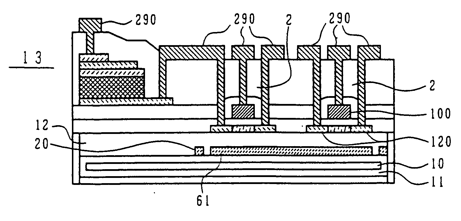
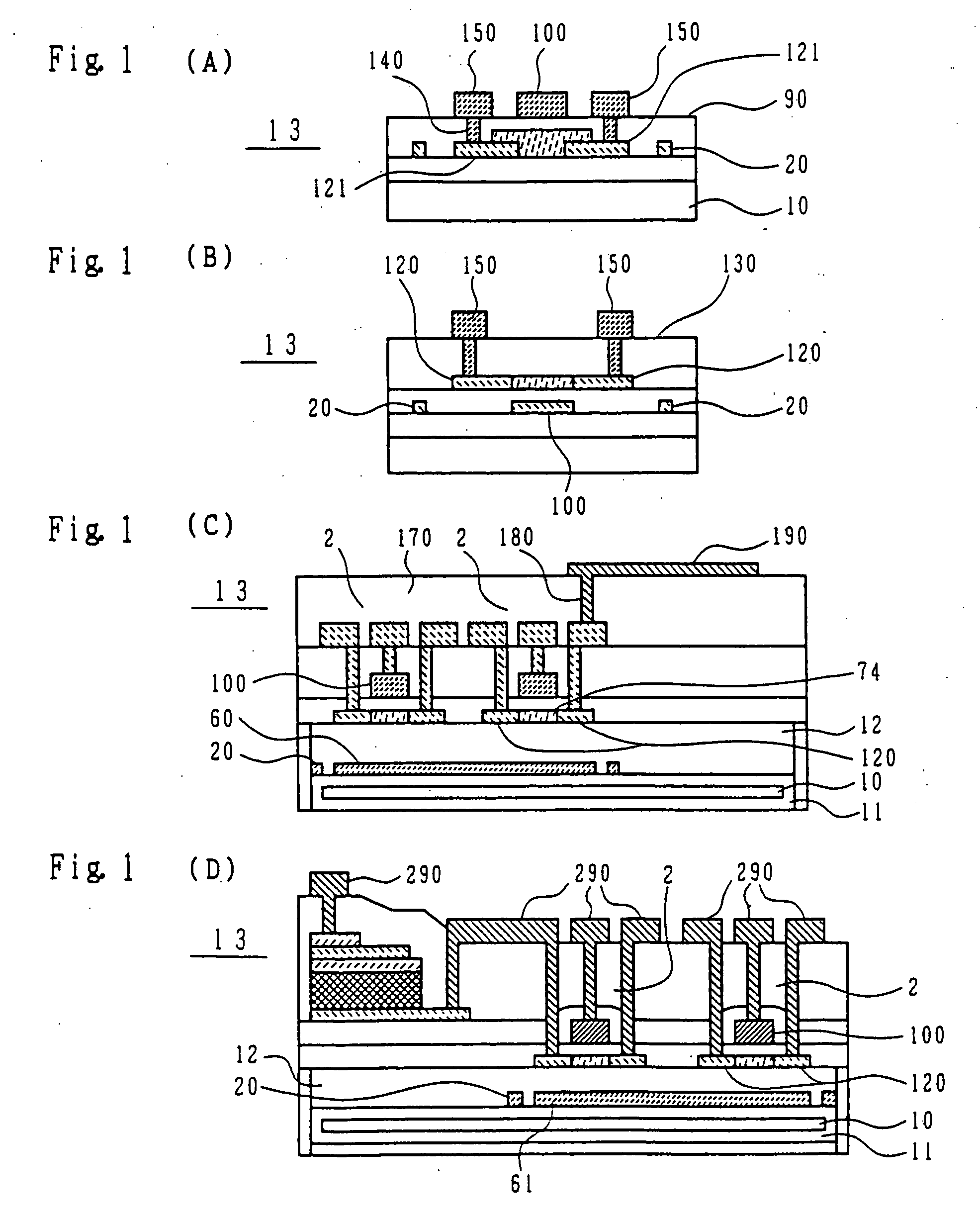
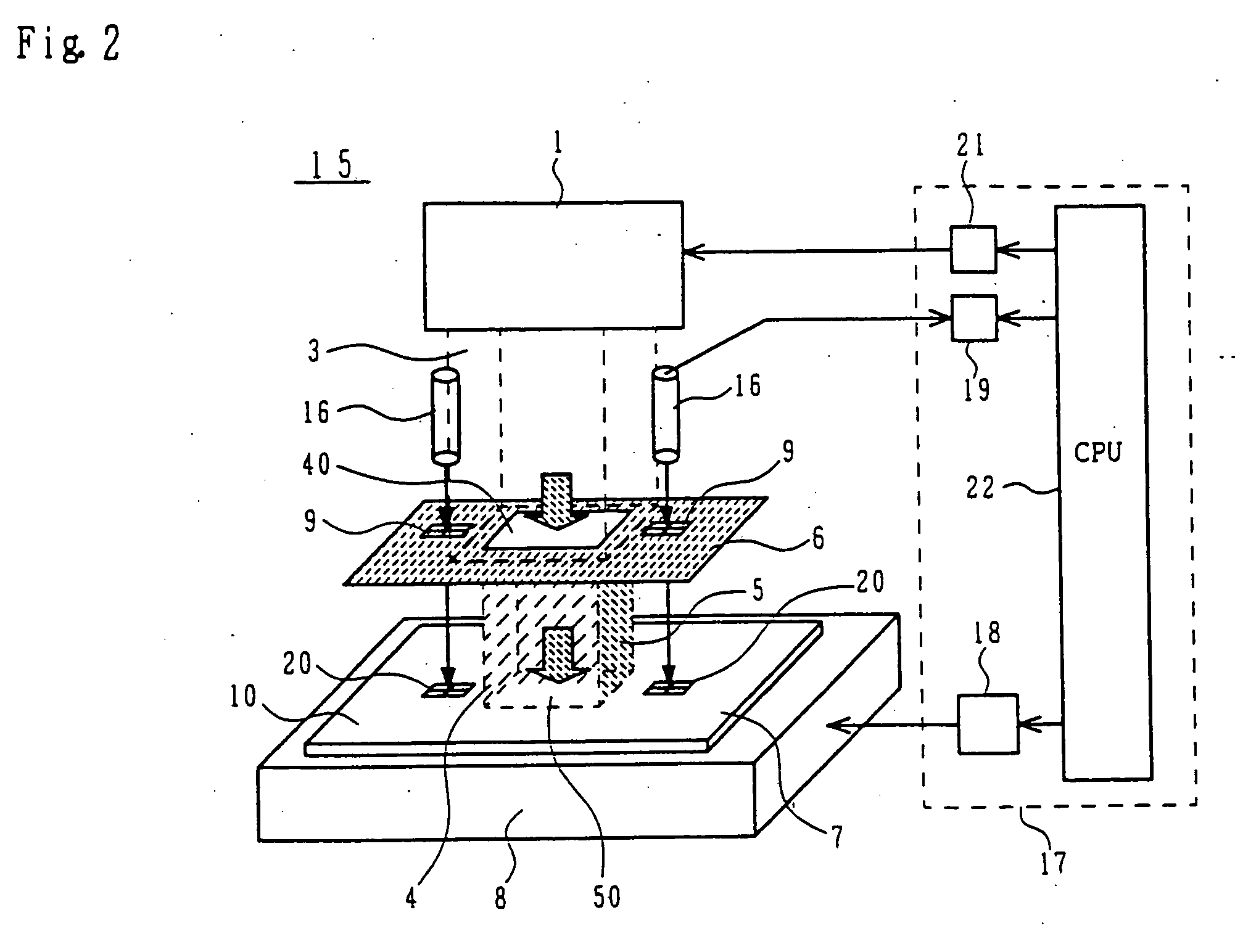
[0052] Specifically, FIG. 1(A) and FIG. 1(B) are drawings showing the configuration of an example of a thin-film transistor 13 according to the present invention.

[0053] These drawings show a thin-film transistor 13 is shown in which, the transistor 13 is formed on a transparent substrate 10, and comprising a gate electrode film 100 and source and drain regions layers 120 and 121, and further wherein an alignment mark 20 is provided, which is made of one and the same constituent material as a constituent material of at least one of the gate electrode film layer 100 and the source and drain region 120, and formed at the same position as at least one of said gate electrode film layer or said source and drain region 120.

[0054] Additionally, another specific example of the present inventio...


PUM

PropertyMeasurementUnit
temperaturesaaaaaaaaaa
thicknessaaaaaaaaaa

Abstract

A thin-film transistor is formed on a transparent substrate and has a gate electrode film layer and a source and drain regions, and further has an alignment mark made of one and the same constituent material as a constituent material of at least one of the gate electrode film layer and source and drain regions and formed at one and the same position as the gate electrode film layer or source and drain region.

Description

BACKGROUND OF THE INVENTION [0001] 1. Field of the Invention [0002] The invention relates to a thin-film transistor, a thin-film transistor manufacturing apparatus, and a method for manufacturing a thin-film transistor, and more particularly it relates to a thin-film transistor and a method for manufacturing a thin-film transistor wherein it is possible to accurately and efficiently position constituent elements of a semiconductor device, and to an electronic apparatus using a thin-film transistor such as an image sensor or an LCD display. [0003] 2. Description of the Related Art [0004] In the past, amorphous silicon thin-film transistors (TFTs) are known as being used as semiconductor devices in input and output apparatuses of contact-type image sensors. [0005] In recent year, an increase in the amount of information and the resultant demand for high resolution and high performance from compact, lightweight portable terminals has focused attention on the polysilicon thin-film trans...

Claims


Application Information

Patent Timeline
Patent Type & Authority Applications(United States)
IPC IPC(8): G02F1/136G02F1/1368G03F7/20H01L21/027H01L21/20H01L21/336H01L21/77H01L21/84H01L23/544H01L27/12H01L27/146H01L29/786
CPCB23K26/04B23K26/0656Y10S438/975H01L21/2026H01L23/544H01L27/1285H01L27/1296H01L29/66757H01L29/66765H01L29/78603H01L29/78633H01L2223/54453H01L2924/0002H01L2924/00B23K26/066H01L21/0262H01L21/02686H01L21/02491H01L21/02422H01L21/02488H01L21/02496H01L21/02532H01L21/02505H01L21/0268H01L21/02691H01L21/02675
Inventor SATOU, YOSHINOBUYUDA, KATSUHISATANABE, HIROSHI
Owner VISTA PEAK VENTURES LLC
Why Eureka
Try Eureka